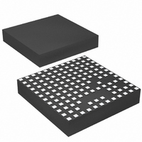
LTM4612IV#PBF Linear Technology, LTM4612IV#PBF Datasheet - Page 8

LTM4612IV#PBF
Manufacturer Part Number
LTM4612IV#PBF
Description
IC BUCK SYNC ADJ 5A 133LGA
Manufacturer
Linear Technology
Series
µModuler
Type
Point of Load (POL) Non-Isolatedr
Datasheet
1.LTM4612EVPBF.pdf
(26 pages)
Specifications of LTM4612IV#PBF
Design Resources
LTM4612 Spice Model
Output
3.3 ~ 15 V
Number Of Outputs
1
Power (watts)
75W
Mounting Type
Surface Mount
Voltage - Input
5 ~ 36 V
Package / Case
133-LGA
1st Output
3.3 ~ 15 VDC @ 5A
Size / Dimension
0.59" L x 0.59" W x 0.11" H (15mm x 15mm x 2.8mm)
Power (watts) - Rated
75W
Operating Temperature
-40°C ~ 125°C
Dc To Dc Converter Type
Non-Inverting/Inverting/Step Up/Step Down
Pin Count
133
Input Voltage
36V
Output Voltage
3.3 to 15V
Switching Freq
940KHz
Output Current
5A
Package Type
LGA
Output Type
Adjustable
Switching Regulator
Yes
Load Regulation
0.6%
Line Regulation
0.3%
Mounting
Surface Mount
Input Voltage (min)
5V
Operating Temperature Classification
Automotive
Lead Free Status / RoHS Status
Lead free / RoHS Compliant
3rd Output
-
2nd Output
-
Lead Free Status / Rohs Status
Compliant
Available stocks
Company
Part Number
Manufacturer
Quantity
Price
LTM4612
pin FuncTions
V
Internally, this pin is connected to V
sion resistor. Different output voltages can be programmed
with an additional resistor between the V
See the Applications Information section.
MARG0 (Pin C12): LSB Logic Input for the Margining
Function. Together with the MARG1 pin, the MARG0 pin
will determine if a margin high, margin low, or no margin
state is applied. The pin has an internal pull-down resistor
of 50k. See the Applications Information section.
MARG1 (Pins C11, D12): MSB Logic Input for the Margin-
ing Function. Together with the MARG0 pin, the MARG1 pin
will determine if a margin high, margin low, or no margin
state is applied. The pins have an internal pull-down resistor
of 50k. See the Applications Information section.
SGND (Pins D9, H12): Signal Ground Pins. These pins
connect to PGND at output capacitor point.
FB
(Pin F12): The Negative Input of the Error Amplifier.
OUT
FB
with a 100k preci-
and SGND pins.
COMP (Pins A11, D11): Current Control Threshold and
Error Amplifier Compensation Point. The current com-
parator threshold increases with this control voltage. The
voltage ranges from 0V to 2.4V with 0.7V corresponding
to zero sense voltage (zero current).
PGOOD (Pin G12): Output Voltage Power Good Indicator.
Open-drain logic output that is pulled to ground when the
output voltage is not within ±10% of the regulation point,
after a 25µs power bad mask timer expires.
RUN (Pins A10, B9): Run Control Pins. A voltage above
1.9V will turn on the module, and below 1V will turn off
the module. A programmable UVLO function can be ac-
complished with a resistor from V
a 5.1V zener to ground. Maximum pin voltage is 5V.
NC (Pins J12, K12, L12): No Connect Pins.
IN
to this pin that is has
4612fa


