APTS012A0X3-SRZ Lineage Power, APTS012A0X3-SRZ Datasheet - Page 5
APTS012A0X3-SRZ
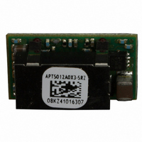
Manufacturer Part Number
APTS012A0X3-SRZ
Description
CONV DC-DC 0.69 5.5V @ 12A SMD
Manufacturer
Lineage Power
Series
Micro TLynx™r
Type
Point of Load (POL) Non-Isolated with Remote On/Offr
Datasheet
1.APTS012A0X3-SRZ.pdf
(26 pages)
Specifications of APTS012A0X3-SRZ
Output
0.69 ~ 5.5V
Number Of Outputs
1
Power (watts)
66W
Mounting Type
Surface Mount
Voltage - Input
4.5 ~ 14V
Package / Case
10-SMD Module
1st Output
0.69 ~ 5.5 VDC @ 12A
Size / Dimension
0.80" L x 0.45" W x 0.33" H (20.3mm x 11.4mm x 8.5mm)
Power (watts) - Rated
66W
Operating Temperature
-40°C ~ 85°C
Efficiency
94%
Approvals
CSA, EN, UL, VDE
Output Power
66 W
Input Voltage Range
4.5 V to 14 V
Output Voltage (channel 1)
0.69 V to 5.5 V
Output Current (channel 1)
12 A
Package / Case Size
SMD
Output Type
Non-Isolated
Output Voltage
0.69 V to 5.5 V
Product
Non-Isolated / POL
Lead Free Status / RoHS Status
Lead free / RoHS Compliant
3rd Output
-
2nd Output
-
Lead Free Status / Rohs Status
Lead free / RoHS Compliant
Other names
555-1129-2
Available stocks
Company
Part Number
Manufacturer
Quantity
Price

Part Number:
APTS012A0X3-SRZ
Manufacturer:
LINEAGE
Quantity:
20 000


Data Sheet
December 2, 2010
Feature Specifications
Unless otherwise indicated, specifications apply over all operating input voltage, resistive load, and temperature
conditions. See Feature Descriptions for additional information.
LINEAGE
Parameter
On/Off Signal Interface
Device is with suffix “4” – Positive Logic (See Ordering
Information)
Device Code with no suffix – Negative Logic (See Ordering
Information)
(On/OFF pin is open collector/drain logic input with
Turn-On Delay and Rise Times
(V
Output voltage overshoot (T
V
With or without maximum external capacitance
Over Temperature Protection
(See Thermal Considerations section)
Sequencing Delay time
Tracking Accuracy
(V
Input Undervoltage Lockout
external pull-up resistor; signal referenced to GND)
Case 1: On/Off input is enabled and then input power is
applied (delay from instant at which V
10% of V
Case 2: Input power is applied for at least one second and
then the On/Off input is enabled (delay from instant at
which Von/Off is enabled until V
Output voltage Rise time (time for V
10% of Vo, set to 90% of Vo, set)
Delay from V
IN
(V
Signal referenced to GND)
Logic High (Module ON)
Logic Low (Module OFF)
Logic High (Module OFF)
Logic Low (Module ON)
IN
IN, min
Turn-on Threshold
Turn-off Threshold
Hysteresis
= V
=V
IN
=V
IN, nom
IN, min
Input High Current
Input High Voltage
Input low Current
Input Low Voltage
Input Low Current
Input Low Voltage
to V
Input High Current
Input High Voltage
IN, min
o, set
POWER
, I
IN, max
to V
to V
O
IN, min
=I
)
IN, max
O, max ,
; I
IN, max
O, min
to application of voltage on SEQ pin
,I
O
V
; open collector or equivalent,
to I
= I
O
O, min
to within ±1% of steady state)
O, max
A
= 25
to I
(Power-Up: 0.5V/ms)
V
(Power-Down: 0.5V/ms)
SEQ
o
o
O, max
= 10% of V
C
4.5 – 14Vdc input; 0.69Vdc to 5.5Vdc output; 12A output current
< V
o
to rise from
)
IN
o
)
= V
IN, min
o, set
12V Micro TLynx
until V
)
o
=
Device
All
All
All
All
All
All
All
All
All
All
All
All
All
All
All
All
All
All
TM
: Non-isolated DC-DC Power Modules
Ts
V
V
Symbol
Tdelay
Tdelay
SEQ
SEQ
Trise
EQ-delay
V
V
V
V
T
I
I
I
I
IH
IH
IL
IL
IH
IH
ref
IL
IL
–V
–V
o
o
V
Min
IN
2.0
―
⎯
⎯
―
―
―
―
―
10
0
– 1
4.45
0.25
Typ
133
4.2
⎯
⎯
⎯
⎯
―
―
―
―
2
2
5
V
V
Max
100
150
3.5
IN, max
3.0
IN,max
25
10
―
―
―
3
1
1
% V
msec
msec
msec
msec
Unit
Vdc
Vdc
Vdc
Vdc
Vdc
mA
mA
mV
mV
µA
μA
°C
V
V
O, set
5
Related parts for APTS012A0X3-SRZ
Image
Part Number
Description
Manufacturer
Datasheet
Request
R

Part Number:
Description:
Manufacturer:
Lineage Power
Datasheet: