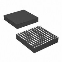
LTM4615IV#PBF Linear Technology, LTM4615IV#PBF Datasheet - Page 3

LTM4615IV#PBF
Manufacturer Part Number
LTM4615IV#PBF
Description
IC SWIT REG BUCK 4A ADJ 144LGA
Manufacturer
Linear Technology
Series
µModuler
Type
Point of Load (POL) Non-Isolatedr
Specifications of LTM4615IV#PBF
Design Resources
LTM4615 Spice Model
Output
0.8 ~ 5 V
Number Of Outputs
3
Power (watts)
12W
Mounting Type
Surface Mount
Voltage - Input
2.38 ~ 5.5 V
Package / Case
144-LGA
1st Output
0.8 ~ 5 VDC @ 4A
2nd Output
0.8 ~ 5 VDC @ 4A
3rd Output
0.8 ~ 5 VDC @ 4A
Size / Dimension
0.59" L x 0.59" W x 0.11" H (15mm x 15mm x 2.8mm)
Power (watts) - Rated
12W
Operating Temperature
-40°C ~ 125°C
Efficiency
95%
Primary Input Voltage
5.5V
No. Of Outputs
3
Output Voltage
5V
Output Current
1.5A
Voltage Regulator Case Style
LGA
No. Of Pins
144
Operating Temperature Range
-40°C To +125°C
Rohs Compliant
Yes
Dc To Dc Converter Type
Step Down
Pin Count
144
Input Voltage
5.5V
Switching Freq
1250KHz
Package Type
LGA
Output Type
Adjustable
Switching Regulator
Yes
Mounting
Surface Mount
Input Voltage (min)
2.375V
Operating Temperature Classification
Automotive
Lead Free Status / RoHS Status
Lead free / RoHS Compliant
Available stocks
Company
Part Number
Manufacturer
Quantity
Price
ELECTRICAL CHARACTERISTICS
SYMBOL
I
I
I
I
ΔV
V
f
ΔV
t
ΔV
t
I
V
I
V
I
V
V
R
ΔV
R
VLDO Section
V
I
I
V
V
operating temperature range, otherwise specifi cations are at T
Per Typical Application Figure 12.
INRUSH(VIN)
Q(VIN)
S(VIN)
OUT(DC)
s
START
SETTLE
OUT(PK)
FB
TRACK
IN(LDO_IN)
IN(SHDN)
TRACK(OFFSET)
TRACK(RANGE)
OUT(AC)
FB
RUN
LDO_IN
BOOST3
BOOST3(UVLO)
FBHI
PGOOD
PGOOD
OUT(LOAD + LINE)
OUT(START)
OUT(LS)
V
OUT
PARAMETER
Input Inrush Current at Start-Up
Input Supply Bias Current
Input Supply Current
Output Continuous Current Range
Load and Line Regulation Accuracy V
Output Ripple Voltage
Output Ripple Voltage Frequency
Turn-On Overshoot
Turn-On Time
Peak Deviation for Dynamic Load
Settling Time for Dynamic Load
Step
Output Current Limit
Voltage at FB Pin
RUN Pin On/Off Threshold
TRACK Pin Current
Offset Voltage
Tracking Input Range
Resistor Between V
PGOOD Range
PGOOD Resistance
Operating Voltage
Operating Current
Shutdown Current
BOOST3 Output Voltage
Undervoltage Lockout
OUT
and FB Pins
CONDITIONS
I
V
V
Shutdown, RUN = 0, V
V
V
V
I
I
C
I
C
Load, TRACK = V
Load: 0% to 50% to 0% of Full Load,
C
Load: 0% to 50% to 0% of Full Load,
V
C
I
TRACK = 0.4V
Open-Drain Pull-Down
(Note 3)
I
EN3 = 0V, LDO_IN = 1.5V
EN3 = 1.2V
OUT
OUT
OUT
OUT
OUT
OUT
IN
IN
IN
IN
IN
OUT
OUT
OUT
OUT
IN
OUT
V
V
V
V
V
V
= 2.375V, V
= 5.5V, V
= 2.375V, V
= 5.5V, V
= 5.5V, V
= 5V, V
= 0A, C
= 0A, C
= 4A, V
= 0A
= 0A, V
= 0mA, V
IN
IN
IN
IN
IN
IN
= 1.5V, 0A to 4A (Note 6)
= 100μF , V
= 100μF , V
= 100μF , V
= 100μF , V
= 5.5V
= 2.375V to 5.5V
= 5V, V
= 3.3V
= 5V
= 5V
The
OUT
IN
OUT
IN
OUT
OUT
OUT
OUT
A
l
OUT
OUT
= 22μF , C
= 5V, V
= 25°C. V
= 1.5V
OUT
OUT
OUT
OUT
IN
IN
denotes the specifi cations which apply over the full internal
= 100μF
= 1.5V
= 1.5V, Switching Continuous
= 1.5V, I
= 1.5V (Note 6)
IN
= 5V, V
= 5V, V
= 1V, EN3 = 1.2V
= 1.5V
= 1.5V, Switching Continuous
= 1.5V, I
= 1.5V, RUN/SS = 10nF ,
= 1.5V, I
and RUN/SS = Float
OUT
IN
OUT
OUT
= 5V
OUT
OUT
IN
= 1.5V
OUT
= 100μF , V
OUT
= 5V, LDO_IN = 1.2V unless otherwise noted.
= 4A
= 1.5V
= 1.5V
= 4A
= 1A Resistive
OUT
= 1.5V,
l
l
l
0.790
0.786
4.96
1.14
MIN
0.6
4.8
0
0
0.35
1.48
±1.0
±1.3
1.25
0.75
4.99
±7.5
TYP
3.2
0.5
0.8
0.8
0.2
0.2
0.6
4.3
28
45
12
20
20
25
10
30
90
7
8
1
5
LTM4615
±1.30
0.807
0.809
MAX
±1.6
5.02
150
0.9
0.8
3.5
5.2
12
20
4
UNITS
mV
3
MHz
4615f
mA
mA
mV
mV
mV
mV
mA
ms
P-P
kΩ
μA
μA
μA
μA
μs
%
%
%
Ω
A
A
A
A
A
V
V
V
V
V
V
V


