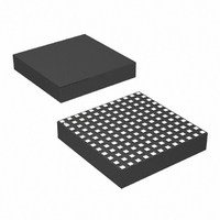
LTM4615IV#PBF Linear Technology, LTM4615IV#PBF Datasheet - Page 4

LTM4615IV#PBF
Manufacturer Part Number
LTM4615IV#PBF
Description
IC SWIT REG BUCK 4A ADJ 144LGA
Manufacturer
Linear Technology
Series
µModuler
Type
Point of Load (POL) Non-Isolatedr
Specifications of LTM4615IV#PBF
Design Resources
LTM4615 Spice Model
Output
0.8 ~ 5 V
Number Of Outputs
3
Power (watts)
12W
Mounting Type
Surface Mount
Voltage - Input
2.38 ~ 5.5 V
Package / Case
144-LGA
1st Output
0.8 ~ 5 VDC @ 4A
2nd Output
0.8 ~ 5 VDC @ 4A
3rd Output
0.8 ~ 5 VDC @ 4A
Size / Dimension
0.59" L x 0.59" W x 0.11" H (15mm x 15mm x 2.8mm)
Power (watts) - Rated
12W
Operating Temperature
-40°C ~ 125°C
Efficiency
95%
Primary Input Voltage
5.5V
No. Of Outputs
3
Output Voltage
5V
Output Current
1.5A
Voltage Regulator Case Style
LGA
No. Of Pins
144
Operating Temperature Range
-40°C To +125°C
Rohs Compliant
Yes
Dc To Dc Converter Type
Step Down
Pin Count
144
Input Voltage
5.5V
Switching Freq
1250KHz
Package Type
LGA
Output Type
Adjustable
Switching Regulator
Yes
Mounting
Surface Mount
Input Voltage (min)
2.375V
Operating Temperature Classification
Automotive
Lead Free Status / RoHS Status
Lead free / RoHS Compliant
Available stocks
Company
Part Number
Manufacturer
Quantity
Price
LTM4615
ELECTRICAL CHARACTERISTICS
SYMBOL
V
V
V
LDO_RHI
I
I
e
V
V
I
V
PGOOD Threshold
Note 1: Stresses beyond those listed under Absolute Maximum Ratings
may cause permanent damage to the device. Exposure to any Absolute
Maximum Rating condition for extended periods may affect device
reliability and lifetime.
Note 2: The LTM4615E is guaranteed to meet performance specifi cations
over the 0°C to 125°C internal operating temperature range. Specifi cations
over the –40°C to 125°C internal operating temperature range are assured
by design, characterization and correlation with statistical process
controls. The LTM4615I is guaranteed to meet specifi cations over the full
internal operating temperature range. Note that the maximum ambient
temperature is determined by specifi c operating conditions in conjunction
with board layout, the rated package thermal resistance and other
environmental factors.
4
operating temperature range, otherwise specifi cations are at T
Per Typical Application Figure 12.
OUT
LIM
IN_EN3
n
FB3
LDO_OUT
DO
IH_EN3
IL_EN3
OL_PGOOD3
PARAMETER
FB3 Internal Reference Voltage
Output Voltage Range
Dropout Voltage
LDO Top Feedback Resistor
Output Current
Output Current Limit
Output Voltage Noise
EN3 Input High Voltage
EN3 Input Low Voltage
EN3 Input Current
PGOOD Low Voltage
Output Threshold
Relative to V
FB3
CONDITIONS
1mA ≤ I
BOOST3 = 5V, 1V ≤ V
V
V
(Note 5)
Frequency = 10Hz to 1MHz, I
1.14V ≤ V
1.14V ≤ V
I
PGOOD3 High to Low
PGOOD3 Low to High
PGOOD3
LDO_IN
EN3
= 1.2V
OUT
= 1.5V, V
= 2mA
The
LDO_IN
LDO_IN
≤ 1.5A, 1.14V ≤ V
A
l
= 25°C. V
denotes the specifi cations which apply over the full internal
≤ 3.5V
≤ 3.5V
FB3
= 0.38V, I
Note 3: Minimum operating voltage required for regulation is:
Note 4: Dropout voltage is the minimum input to output differential needed
to maintain regulation at a specifi ed output current. In dropout the output
voltage will be equal to V
Note 5: The IC has overtemperature protection that is intended to protect
the device during momentary overload conditions. Junction temperatures
will exceed 125°C when overtemperature is activated. Continuous
overtemperature activation can impair long-term reliability.
Note 6: See output current derating curves for different V
OUT
V
≤ 2.59V
IN
IN
= 5V, LDO_IN = 1.2V unless otherwise noted.
≥ V
LOAD
LDO_IN
OUT
OUT(MIN)
= 1.5A (Note 4)
= 1A
≤ 3.5V,
+ V
DROPOUT
IN
– V
DROPOUT
l
l
l
0.397
0.395
4.96
MIN
.
–14
0.4
1.5
–1
–4
1
4.99
TYP
100
300
–12
0.4
0.4
2.5
0.1
–3
IN
0.404
0.405
MAX
, V
5.02
250
–10
2.6
0.4
0.4
–2
1
OUT
and T
UNITS
μRMS
4615f
mV
A
kΩ
μA
.
%
%
V
V
V
A
A
V
V
V


