LTM4612MPV#PBF Linear Technology, LTM4612MPV#PBF Datasheet - Page 7
LTM4612MPV#PBF
Manufacturer Part Number
LTM4612MPV#PBF
Description
IC BUCK SYNC ADJ 5A 133LGA
Manufacturer
Linear Technology
Series
µModuler
Type
Point of Load (POL) Non-Isolatedr
Datasheet
1.LTM4612EVPBF.pdf
(26 pages)
Specifications of LTM4612MPV#PBF
Design Resources
LTM4612 Spice Model
Output
3.3 ~ 15 V
Number Of Outputs
1
Power (watts)
75W
Mounting Type
Surface Mount
Voltage - Input
5 ~ 36 V
Package / Case
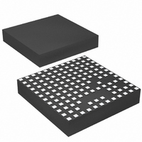
133-LGA
1st Output
3.3 ~ 15 VDC @ 5A
Size / Dimension
0.59" L x 0.59" W x 0.11" H (15mm x 15mm x 2.8mm)
Power (watts) - Rated
75W
Operating Temperature
-55°C ~ 125°C
Lead Free Status / RoHS Status
Lead free / RoHS Compliant
3rd Output
-
2nd Output
-
Available stocks
Company
Part Number
Manufacturer
Quantity
Price


pin FuncTions
V
tween these pins and PGND pins. Recommend placing
input decoupling capacitance directly between V
and PGND pins.
PGND (Bank 2): Power Ground Pins for Both Input and
Output Returns.
V
between these pins and PGND pins. Recommend placing out-
put decoupling capacitance directly between these pins and
GND pins (see the LTM4612 Pin Configuration below).
V
citors between V
current and reduce the input ripple further.
DRV
nect to INTV
They can be biased up to 6V from an external supply with
about 50mA capability. This improves efficiency at the
higher input voltages by reducing power dissipation in
the module.
INTV
the 5V internal regulator.
PLLIN (Pin A8): External Clock Synchronization Input to the
Phase Detector. This pin is internally terminated to SGND
with a 50k resistor. Apply a clock above 2V and below
INTV
OUT
IN
D
(Pins B7, C7): Top FET Drain Pins. Add more capa-
(Bank 1): Power Input Pins. Apply input voltage be-
CC
CC
CC
(Bank 3): Power Output Pins. Apply output load
. See the Applications Information section.
(Pins C10, E11, E12): These pins normally con-
(Pin A7): This pin is for additional decoupling of
CC
for powering the internal MOSFET drivers.
D
and ground to handle the input RMS
(See Package Description for Pin Assignments)
BANK 1
BANK 2
BANK 3
PGND
V
OUT
V
IN
A
B
C
D
E
F
G
H
J
K
L
M
1
133-LEAD (15mm × 15mm × 2.8mm)
2
LTM4612 Pin Configuration
3
IN
4
pins
LGA PACKAGE
TOP VIEW
5 6
7
V
8
FCB (Pin M12): Forced Continuous Input. Connect this pin
to SGND to force continuous synchronization operation at
low load, to INTV
tion at low load or to a resistive divider from a secondary
output when using a secondary winding.
TRACK/SS (Pin A9): Output Voltage Tracking and Soft-Start
Pin. When the module is configured as a master output,
then a soft-start capacitor is placed on this pin to ground
to control the master ramp rate. A soft-start capacitor can
be used for soft-start turn-on as a standalone regulator.
Slave operation is performed by putting a resistor divider
from the master output to the ground, and connecting the
center point of the divider to this pin. See the Applications
Information section.
MPGM (Pins A12, B11): Programmable Margining Input.
A resistor from these pins to ground sets a current that is
equal to 1.18V/R. This current multiplied by 10k will equal
a value in millivolts that is a percentage of the 0.6V refer-
ence voltage. See the Applications Information section.
To parallel LTM4612s, each requires an individual MPGM
resistor. Do not tie MPGM pins together.
f
Output. An external resistor can be placed from this pin to
ground to increase frequency. This pin can be decoupled
with a 1000pF capacitor. See the Applications Information
section for frequency adjustment.
D
SGND
SET
9
10 11
(Pin B12): Frequency Set Internally to 850kHz at 12V
12
f
MARG0
MARG1
DRV
V
PGOOD
SGND
NC
NC
NC
FCB
SET
FB
CC
CC
to enable discontinuous mode opera-
LTM4612
4612fa
Related parts for LTM4612MPV#PBF
Image
Part Number
Description
Manufacturer
Datasheet
Request
R

Part Number:
Description:
CD ROM LINEARVIEW DATASHEETS
Manufacturer:
Linear Technology

Part Number:
Description:
Standalone Linear Li-Ion Battery Charger with Thermal Regulation in ThinSOT
Manufacturer:
Linear Technology Corporation
Datasheet:
Part Number:
Description:
Low noise, high frequency, 8th order linear phase lowpass filter
Manufacturer:
Linear Technology Corporation
Datasheet:
Part Number:
Description:
Manufacturer:
Linear Technology Corporation
Datasheet:
Part Number:
Description:
Manufacturer:
Linear Technology Corporation
Datasheet:
Part Number:
Description:
Manufacturer:
Linear Technology Corporation
Datasheet:
Part Number:
Description:
Manufacturer:
Linear Technology Corporation
Datasheet:
Part Number:
Description:
Manufacturer:
Linear Technology Corporation
Datasheet:
Part Number:
Description:
Manufacturer:
Linear Technology Corporation
Datasheet:
Part Number:
Description:
Manufacturer:
Linear Technology Corporation
Datasheet:
Part Number:
Description:
Dual and Quad, JFET Input Precision High Speed Op Amps
Manufacturer:
Linear Technology Corporation
Datasheet:
Part Number:
Description:
Manufacturer:
Linear Technology Corporation
Datasheet:
Part Number:
Description:
1, 2, 6 and 8 Channel, 10-Bit Serial I/O Data Acquisition Systems
Manufacturer:
Linear Technology Corporation
Datasheet:
Part Number:
Description:
Manufacturer:
Linear Technology Corporation
Datasheet:
Part Number:
Description:
Universal dual filter building block
Manufacturer:
Linear Technology Corporation
Datasheet: