HW-USB-II-G Xilinx Inc, HW-USB-II-G Datasheet - Page 15
HW-USB-II-G
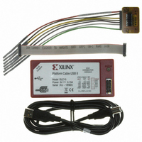
Manufacturer Part Number
HW-USB-II-G
Description
PLATFORM CABLE USB II
Manufacturer
Xilinx Inc
Datasheet
1.HW-USB-II-G.pdf
(35 pages)
Specifications of HW-USB-II-G
Accessory Type
USB Platform Cable
For Use With/related Products
Xilinx FPGA, CPLDS, Platform Flash PROMs, XC18V00 PROMs, System ACE MPM
Lead Free Status / RoHS Status
Lead free / RoHS Compliant
Other names
122-1572
Available stocks
Company
Part Number
Manufacturer
Quantity
Price
Company:

Part Number:
HW-USB-II-G
Manufacturer:
APEC
Quantity:
4 000


Target System Connections
This section provides examples of the various configuration topologies supported by Platform Cable USB II. Each example
incorporates the 2-mm connector (see
provide a functional relationship between the cable interface and the target devices.
Note:
JTAG and Slave Serial
Multiple devices can be cascaded when using either a JTAG or slave-serial topology in target systems.
Figure 17, page 17
Platform Cable USB II provides a multi-use signal on its target interface connector called pseudo ground (PGND). The
PGND pin is connected to an open-drain driver (see
behavior of PGND is determined by the host application connected to the cable. In iMPACT, PGND is active-Low during
JTAG, Slave Serial and SPI operations (for example, programming, configuration, read back, etc.) and high-Z when the cable
is idle.
Figure 16, page 16
the select (S) term on a set of multiplexers that switch between the primary configuration source and the cable. When PGND
is active-Low, the cable drives the JTAG chain. When PGND is high-Z, the primary configuration source drives the JTAG
chain. This capability allows Platform Cable USB II to remain attached to the target system while remaining isolated from the
primary configuration source. A similar scheme can be used with Slave Serial topologies.
PGND control is available only in iMPACT versions 10.1 and later. PGND remains high-Z in earlier versions of iMPACT and
in Xilinx design tools where the PGND signal is not supported.
The DONE pin on FPGAs can be programmed to be an open-drain or active driver. For cascaded Slave Serial topologies,
an external pull-up resistor should be used, and all devices should be programmed for open-drain operation.
X-Ref Target - Figure 15
Notes:
1.
2.
DS593 (v1.2.1) March 17, 2011
Example implies that V
appropriate JTAG voltage-supply levels.
Attach the following 2-mm connector pins to digital ground: 3, 5, 7, 9, and 11.
GND
Signal integrity is not considered in these examples. Refer to
V
TDO
TMS
TCK
REF
TDI
(2 )
10
2
8
4
6
*
V
CCAUX (1)
shows a typical use of PGND as a control signal to manage a target system’s JTAG chain. PGND drives
show typical routing for JTAG and Slave Serial topologies, respectively.
2-mm Connector
CCO
, V
CCJ
, and V
TDI
TMS
Figure 15: Example of JTAG Chain Topology
Target Interface Connectors, page
CCAUX
PROM
ISP
TCK
for various devices are set to the same voltage. Refer to the device data sheet for the
TDO
Pseudo Ground Signal, page
www.xilinx.com
Signal Integrity, page 27
TDI
TMS
FPGA
14) as the cable interface. Diagrams in this section
TCK
TDO
22); hence, it is either Low or high-Z. The
for details on buffering and termination.
TDI
TMS
CPLD
Platform Cable USB II
TCK
Figure 15
TDO
DS593_15_011508
and
15
Related parts for HW-USB-II-G
Image
Part Number
Description
Manufacturer
Datasheet
Request
R

Part Number:
Description:
PLATFORM CABLE USB
Manufacturer:
Xilinx Inc
Datasheet:

Part Number:
Description:
IC CABLE
Manufacturer:
Xilinx Inc
Datasheet:

Part Number:
Description:
BOARD ADAPTER AND FLY LEADS
Manufacturer:
Xilinx Inc
Datasheet:

Part Number:
Description:
XLXHW-LICENSE-DONGLE-USB-G USB DONGLE OP
Manufacturer:
Xilinx Inc

Part Number:
Description:
IC CPLD .8K 36MCELL 44-VQFP
Manufacturer:
Xilinx Inc
Datasheet:

Part Number:
Description:
IC CPLD 72MCRCELL 10NS 44VQFP
Manufacturer:
Xilinx Inc
Datasheet:

Part Number:
Description:
IC CPLD 1.6K 72MCELL 64-VQFP
Manufacturer:
Xilinx Inc
Datasheet:

Part Number:
Description:
IC CR-II CPLD 64MCELL 44-VQFP
Manufacturer:
Xilinx Inc
Datasheet:

Part Number:
Description:
IC CPLD 1.6K 72MCELL 100-TQFP
Manufacturer:
Xilinx Inc
Datasheet:

Part Number:
Description:
IC CR-II CPLD 64MCELL 56-BGA
Manufacturer:
Xilinx Inc
Datasheet:

Part Number:
Description:
IC CPLD 72MCRCELL 7.5NS 44VQFP
Manufacturer:
Xilinx Inc
Datasheet:
Part Number:
Description:
IC CR-II CPLD 64MCELL 100-VQFP
Manufacturer:
Xilinx Inc
Datasheet:
Part Number:
Description:
IC CPLD 1.6K 72MCELL 100-TQFP
Manufacturer:
Xilinx Inc
Datasheet:

Part Number:
Description:
IC CPLD 72MCRCELL 7.5NS 64VQFP
Manufacturer:
Xilinx Inc
Datasheet:
Part Number:
Description:
IC CPLD 1.6K 72MCELL 100-TQFP
Manufacturer:
Xilinx Inc
Datasheet: