HW-USB-II-G Xilinx Inc, HW-USB-II-G Datasheet - Page 30
HW-USB-II-G
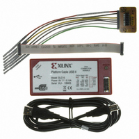
Manufacturer Part Number
HW-USB-II-G
Description
PLATFORM CABLE USB II
Manufacturer
Xilinx Inc
Datasheet
1.HW-USB-II-G.pdf
(35 pages)
Specifications of HW-USB-II-G
Accessory Type
USB Platform Cable
For Use With/related Products
Xilinx FPGA, CPLDS, Platform Flash PROMs, XC18V00 PROMs, System ACE MPM
Lead Free Status / RoHS Status
Lead free / RoHS Compliant
Other names
122-1572
Available stocks
Company
Part Number
Manufacturer
Quantity
Price
Company:

Part Number:
HW-USB-II-G
Manufacturer:
APEC
Quantity:
4 000


Table 6: JTAG/SPI/Slave Serial Port: 2-mm Connector Signals (Cont’d)
DS593 (v1.2.1) March 17, 2011
Number
Pin
10
13
14
10
13
14
4
6
8
4
6
Configuration
PGND
JTAG
HALT
TDI
–
–
–
–
–
–
–
–
Programming
MODE
PGND
MISO
MOSI
SCK
SPI
WP
SS
–
–
–
–
–
(1)
Configuration
Slave-Serial
PROG
CCLK
www.xilinx.com
–
–
–
–
–
–
–
–
–
Direction
Out
Out
Out
Out
Out
Out
Out
Out
Out
In
–
(2)
JTAG Test Data In. This pin outputs the
serial data stream transmitted to the TDI pin
on the first device in a JTAG chain.
JTAG Pseudo Ground. Use of this pin is
optional. PGND is pulled Low during JTAG
operations; otherwise, it is high-Z. This pin is
connected to an open-drain driver and
requires a pull-up resistor on the target
system.
JTAG Halt. Use of this pin is optional. Host
applications can customize the behavior of
this signal. See
iMPACT, page
SPI Select. This pin is the active-Low SPI
chip select signal and should be connected
to the S
SPI Clock. This pin is the clock signal for
SPI operations and should be connected to
the C
SPI Master-Input, Slave-Output. This pin
is the target serial output data stream and
should be connected to the Q
SPI flash device.
SPI Master-Output Slave-Input. This pin
outputs the target serial input data stream
for SPI operations and should be connected
to the D
SPI Pseudo Ground. PGND is pulled Low
during SPI operations; otherwise, it is high-
Z. When connected to PROG_B on an
FPGA, the FPGA will high-Z its SPI signals
while the cable is programming the SPI
flash. This pin is connected to an open-drain
driver and requires a pull-up resistor on the
target system.
SPI Write Protect. This pin is reserved for
future use. Do not connect for SPI
programming.
Slave Serial Configuration Reset. This pin
is used to force a reconfiguration of the
target FPGA(s) and should be connected to
the PROG_B pin of the target FPGA for a
single-device system, or to the PROG_B pin
of all FPGAs in parallel in a daisy-chain
configuration.
Slave Serial Configuration Clock. FPGAs
load one configuration bit per CCLK cycle in
Slave Serial mode. CCLK should be
connected to the CCLK pin on the target
FPGA for single-device configuration, or to
the CCLK pin of all FPGAs in parallel in a
daisy-chain configuration.
(1)
(4)
(1)
(1)
pin on the SPI flash PROM.
pin on the SPI flash device.
pin on the SPI flash device.
(4)
22.
Description
HALT_INIT_WP Signal in
Platform Cable USB II
(1)
pin on the
30
Related parts for HW-USB-II-G
Image
Part Number
Description
Manufacturer
Datasheet
Request
R

Part Number:
Description:
PLATFORM CABLE USB
Manufacturer:
Xilinx Inc
Datasheet:

Part Number:
Description:
IC CABLE
Manufacturer:
Xilinx Inc
Datasheet:

Part Number:
Description:
BOARD ADAPTER AND FLY LEADS
Manufacturer:
Xilinx Inc
Datasheet:

Part Number:
Description:
XLXHW-LICENSE-DONGLE-USB-G USB DONGLE OP
Manufacturer:
Xilinx Inc

Part Number:
Description:
IC CPLD .8K 36MCELL 44-VQFP
Manufacturer:
Xilinx Inc
Datasheet:

Part Number:
Description:
IC CPLD 72MCRCELL 10NS 44VQFP
Manufacturer:
Xilinx Inc
Datasheet:

Part Number:
Description:
IC CPLD 1.6K 72MCELL 64-VQFP
Manufacturer:
Xilinx Inc
Datasheet:

Part Number:
Description:
IC CR-II CPLD 64MCELL 44-VQFP
Manufacturer:
Xilinx Inc
Datasheet:

Part Number:
Description:
IC CPLD 1.6K 72MCELL 100-TQFP
Manufacturer:
Xilinx Inc
Datasheet:

Part Number:
Description:
IC CR-II CPLD 64MCELL 56-BGA
Manufacturer:
Xilinx Inc
Datasheet:

Part Number:
Description:
IC CPLD 72MCRCELL 7.5NS 44VQFP
Manufacturer:
Xilinx Inc
Datasheet:
Part Number:
Description:
IC CR-II CPLD 64MCELL 100-VQFP
Manufacturer:
Xilinx Inc
Datasheet:
Part Number:
Description:
IC CPLD 1.6K 72MCELL 100-TQFP
Manufacturer:
Xilinx Inc
Datasheet:

Part Number:
Description:
IC CPLD 72MCRCELL 7.5NS 64VQFP
Manufacturer:
Xilinx Inc
Datasheet:
Part Number:
Description:
IC CPLD 1.6K 72MCELL 100-TQFP
Manufacturer:
Xilinx Inc
Datasheet: