MCP6XXXDM-FLTR Microchip Technology, MCP6XXXDM-FLTR Datasheet - Page 14
MCP6XXXDM-FLTR
Manufacturer Part Number
MCP6XXXDM-FLTR
Description
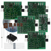
KIT DEMO BOARD ACTIVE FILTER
Manufacturer
Microchip Technology
Datasheet
1.MCP6XXXDM-FLTR.pdf
(46 pages)
Specifications of MCP6XXXDM-FLTR
Main Purpose
Filters, Active - Bandpass, Highpass, Lowpass
Embedded
Yes, MCU, 8-Bit
Utilized Ic / Part
MCP6271
Primary Attributes
Cascadable PCBs, Single Supply
Secondary Attributes
Bessel, Butterworth, and Chebyshev, with Order 1 ~ 8
Processor To Be Evaluated
MCP6271
Lead Free Status / RoHS Status
Not applicable / Not applicable
Lead Free Status / RoHS Status
Lead free / RoHS Compliant, Not applicable / Not applicable
Available stocks
Company
Part Number
Manufacturer
Quantity
Price
Company:

Part Number:
MCP6XXXDM-FLTR
Manufacturer:
MICROCHIP
Quantity:
12 000
Part Number:
MCP6XXXDM-FLTR
Manufacturer:
MICROCHIP/微芯
Quantity:
20 000


2.4
DS51614A-page 10
V
DD
/2 FILTER SECTION SET-UP
The user provides the supply voltages, which need to be in the allowed range for the
installed op amps. Any of Microchip’s op amps that operate below 5.5V can be used;
higher voltage parts can be accommodated (see Section 4.2 “Power Supplies”). Five
MCP6271 op amps are included in the accessory bag for convenience.
The power lines are bypassed by 1.0 µF capacitors at each board input. The op amps
also have 0.1 µF local bypass capacitors.
Figure 2-2 gives the circuit diagram for the V
voltage (V
at INT) by the on-board op amp (U
flexibility in setting up a filter circuit.
FIGURE 2-2:
The V
either a PDIP-8 or SOIC-8 package:
• PDIP-8 packages are inserted into the DIP-8 socket above the U1 label
• SOIC-8 packages can be accommodated; see Section 4.6 “Using 8-Pin SOIC
• Only one op amp can be connected at a time
Select the mid-supply power source by setting jumper JP1 to (see Figure 2-3):
• Internal V
• External V
The headers P1 and J1 on the left of the board are unpopulated (see Figure 2-3):
• The test points TP1 through TP5 provide connections for the same voltages
• P1 and J1 can be populated by the user, if desired, to connect to another (user
Op Amps”
- Op amp U1 drives the V
- The V
- Op amp U1 has no load
- The V
provided) board on the left
TP4)
V
GND
GND
GND
DD
DD
V
V
DD
/2
/2 Filter Section PCB is shown in Figure 2-3. The single op amp U1 can have
IN
DD
DD
DD
DD
DD
/2) to be set by an external power supply (JP
/2 line must be disconnected from any power supply (at P1 or TP4)
/2 line must be connected to an external supply voltage (at P1 or
/2 (INT on bottom)
/2 (EXT on top, as shown)
P
J
1
1
V
DD
C
1.0 µF
2
/2 Filter Section Circuit.
C
1.0 µF
TP
V
1
TP
GND
DD
IN
20 kΩ
0.1 µF
1
2
/2 line on all of the PCBs
C
R
3
1
1
). The headers and test points allow the user
R
20 kΩ
JP
2
1
DD
/2 Filter Section. It allows the mid-supply
C
0.1 µF
4
EXT
INT
U
MCP6271
1
1
© 2006 Microchip Technology Inc.
at EXT), or internally (JP
TP
V
TP
V
TP
TP
GND
DD
DD
3
4
5
5
/2
P
J
2
2
V
V
GND
GND
V
GND
DD
DD
OUT
/2
1
Related parts for MCP6XXXDM-FLTR
Image
Part Number
Description
Manufacturer
Datasheet
Request
R

Part Number:
Description:
Manufacturer:
Microchip Technology Inc.
Datasheet:
Part Number:
Description:
Manufacturer:
Microchip Technology Inc.
Datasheet:
Part Number:
Description:
Manufacturer:
Microchip Technology Inc.
Datasheet:
Part Number:
Description:
Manufacturer:
Microchip Technology Inc.
Datasheet:
Part Number:
Description:
Manufacturer:
Microchip Technology Inc.
Datasheet:
Part Number:
Description:
Manufacturer:
Microchip Technology Inc.
Datasheet:
Part Number:
Description:
Manufacturer:
Microchip Technology Inc.
Datasheet:
Part Number:
Description:
Manufacturer:
Microchip Technology Inc.
Datasheet: