MCP3905EV Microchip Technology, MCP3905EV Datasheet - Page 11
MCP3905EV
Manufacturer Part Number
MCP3905EV
Description
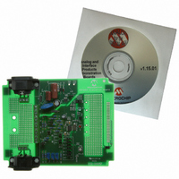
BOARD DEMO FOR MCP3905
Manufacturer
Microchip Technology
Type
Other Power Managementr
Specifications of MCP3905EV
Main Purpose
Power Management, Energy/Power Meter
Embedded
No
Utilized Ic / Part
MCP3905/6
Primary Attributes
1-Phase, 120/220 VAC, On Board Transformerless AC/DC 5V Supply
Silicon Manufacturer
Microchip
Silicon Core Number
MCP3905A
Kit Application Type
Power Management
Application Sub Type
Energy Meter
Kit Contents
Board & Design Guides
Product
Power Management Modules
Lead Free Status / RoHS Status
Contains lead / RoHS non-compliant
Secondary Attributes
-
Lead Free Status / Rohs Status
Lead free / RoHS Compliant
For Use With/related Products
MCP3905
Lead Free Status / RoHS Status
Lead free / RoHS Compliant, Contains lead / RoHS non-compliant


3.0
The descriptions of the pins are listed in
TABLE 3-1:
3.1
DV
within the MCP3905/06.
DV
should be maintained to 5V ±10% for specified
operation. Please refer to Section 5.0 “Applications
Information”.
3.2
HPF controls the state of the high-pass filter in both
input channels. A logic ‘1’ enables both filters,
removing any DC offset coming from the system or the
device. A logic ‘0’ disables both filters, allowing DC
voltages to be measured.
© 2009 Microchip Technology Inc.
DD
DD
MCP3905/06
SSOP-24
is the power supply pin for the digital circuitry
requires appropriate bypass capacitors and
PIN DESCRIPTIONS
Digital V
High-Pass Filter Input Logic Pin
(HPF)
10
11
12
13
14
15
16
17
18
19
20
21
22
23
24
1
2
3
4
5
6
7
8
9
PIN FUNCTION TABLE
DD
(DV
REFIN/OUT
Symbol
HF
MCLR
OSC1
OSC2
F
F
CH0+
CH1+
DV
A
D
AV
CH0-
CH1-
NEG
HPF
DD
OUT1
OUT0
NC
NC
G1
G0
GND
F2
F1
F0
GND
OUT
DD
DD
)
Table
Digital Power Supply Pin
High-Pass Filters Control Logic Pin
Analog Power Supply Pin
No Connect
Master Clear Logic Input Pin
Analog Ground Pin, Return Path for internal analog circuitry
Gain Control Logic Input Pin
Gain Control Logic Input Pin
Oscillator Crystal Connection Pin or Clock Input Pin
Oscillator Crystal Connection Pin or Clock Output Pin
No Connect
Negative Power Logic Output Pin
Digital Ground Pin, Return Path for Internal Digital Circuitry
High-Frequency Logic Output Pin (Intended for Calibration)
Differential Mechanical Counter Logic Output Pin
Differential Mechanical Counter Logic Output Pin
Non-Inverting Analog Input Pin for Channel 0 (Current Channel)
Inverting Analog Input Pin for Channel 0 (Current Channel)
Inverting Analog Input Pin for Channel 1 (Voltage Channel)
Non-Inverting Analog Input Pin for Channel 1 (Voltage Channel)
Voltage Reference Input/Output Pin
Frequency Control for HF
Frequency Control for F
Frequency Control for F
3-1.
3.3
AV
within the MCP3905/06.
AV
should be maintained to 5V ±10% for specified
operation. Please refer to Section 5.0 “Applications
Information”.
OUT0/1
OUT0/1
OUT
DD
DD
is the power supply pin for the analog circuitry
Logic Input Pin
requires appropriate bypass capacitors and
Logic Input Pin
Logic Input Pin
Analog V
Definition
DD
MCP3905/06
(AV
DD
)
DS21948E-page 11
Related parts for MCP3905EV
Image
Part Number
Description
Manufacturer
Datasheet
Request
R

Part Number:
Description:
Manufacturer:
Microchip Technology Inc.
Datasheet:
Part Number:
Description:
Manufacturer:
Microchip Technology Inc.
Datasheet:
Part Number:
Description:
Manufacturer:
Microchip Technology Inc.
Datasheet:
Part Number:
Description:
Manufacturer:
Microchip Technology Inc.
Datasheet:
Part Number:
Description:
Manufacturer:
Microchip Technology Inc.
Datasheet:
Part Number:
Description:
Manufacturer:
Microchip Technology Inc.
Datasheet:
Part Number:
Description:
Manufacturer:
Microchip Technology Inc.
Datasheet:
Part Number:
Description:
Manufacturer:
Microchip Technology Inc.
Datasheet: