ATDVK90CAN1 Atmel, ATDVK90CAN1 Datasheet - Page 35
ATDVK90CAN1
Manufacturer Part Number
ATDVK90CAN1
Description
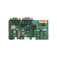
KIT DEV FOR AT90CAN128 MCU
Manufacturer
Atmel
Specifications of ATDVK90CAN1
Main Purpose
*
Embedded
*
Utilized Ic / Part
AT90CAN AVR Devices
Primary Attributes
*
Secondary Attributes
*
Processor To Be Evaluated
AT90CAN
Data Bus Width
8 bit
Interface Type
RS-232, SPI, TWI
Core Architecture
AVR
Core Sub-architecture
AVR UC3
Kit Contents
Board, AT90CAN128 Sample Microcontroller, 9V Battery Power Cable, CD-ROM, Manuals
Features
RS232, CAN, LIN, SPI & TWI Serial Interface
Rohs Compliant
Yes
Lead Free Status / RoHS Status
Contains lead / RoHS non-compliant
Available stocks
Company
Part Number
Manufacturer
Quantity
Price
Company:

Part Number:
ATDVK90CAN1
Manufacturer:
Atmel
Quantity:
135


3.8.1
3.8.2
3.8.3
3.8.4
DVK90CAN1 Hardware User Guide
Supply Voltage from STK500
Analog Reference Voltage from STK500
EXP.CON 0 & EXP.CON 1 Connectors
Main Clock from STK500
The AVR supply voltage coming from STK500 (VTG) can also be controlled from AVR
Studio®.
n Need of the optional expended connectors EXP.CON 0 & EXP.CON 1 (J13 & J14),
n Need of the optional specific decoupling capacitors (C14 & C15 = 100 nF),
n The supply voltage coming from STK500 is controlled by power supply circuitry of
The AVR Analog Reference Voltage coming from STK500 (REF) can also be controlled
from AVR Studio®.
n Need of the optional expended connectors EXP.CON 0 & EXP.CON 1 (J13 & J14),
n Need of the optional specific decoupling capacitor (C16 = 100 nF),
n Refer to Table 3-5 . ANA REF Setting to configure.
Figure 3-41 . EXP.CON 0 and EXP.CON 1 Connectors
The AVR clock frequency (external) coming from STK500 (XT1/XT2) can also be
controlled from AVR Studio® .
n Need of the optional expended connectors EXP.CON 0 & EXP.CON 1 (J13 & J14),
n Refer to Table 3-2 . Main Clock Setting to configure XTAL1 & XTAL2.
the DVK90CAN1. Refer to Table 3-1 . Power Supply (1) Setting to configure.
n.c. (AUXI0 )
n.c. (CT7 )
n.c. (CT5 )
n.c. (CT3 )
n.c. (CT1 )
NRST
GND
GND
GND
PG1
VTG
PC7
PC5
PC3
PC1
PA7
PA5
PA3
PA1
n.c.
EXP. CON 0
11 12
13 14
15 16
17 18
19 20
21 22
23 24
25 26
27 28
29 30
31 32
33 34
35 36
37 38
39 40
1 2
3 4
5 6
7 8
9 10
GND
n.c. ( AUXO0)
n.c. ( CT6)
n.c. ( CT4)
n.c. ( CT2)
n.c. ( BSEL2)
REF
PG2
PG0
GND
VTG
PC6
PC4
PC2
PC0
PA6
PA4
PA2
PA0
GND
Top View
n.c. (DATA7)
n.c. (DATA5)
n.c. (DATA3)
n.c. (DATA1)
n.c. (AUXI1 )
n.c. ( SCK)
n.c. (SI)
GND
GND
GND
VTG
PB7
PB5
PB3
PB1
PD7
PD5
PD3
PD1
XT1
EXP. CON 1
11 12
13 14
15 16
17 18
19 20
21 22
23 24
25 26
27 28
29 30
31 32
33 34
35 36
37 38
39 40
1 2
3 4
5 6
7 8
9 10
GND
n.c. ( AUXO1)
n.c. ( DATA6)
n.c. ( DATA4)
n.c. ( DATA2)
n.c. ( DATA0)
n.c. ( S O)
n.c. ( CS)
XT2
VTG
GND
PB6
PB4
PB2
PB0
PD6
PD4
PD2
PD0
GND
Using the DVK90CAN1
4381A–AVR–Sept 04
page 33
Related parts for ATDVK90CAN1
Image
Part Number
Description
Manufacturer
Datasheet
Request
R

Part Number:
Description:
DEV KIT FOR AVR/AVR32
Manufacturer:
Atmel
Datasheet:

Part Number:
Description:
INTERVAL AND WIPE/WASH WIPER CONTROL IC WITH DELAY
Manufacturer:
ATMEL Corporation
Datasheet:
Part Number:
Description:
Low-Voltage Voice-Switched IC for Hands-Free Operation
Manufacturer:
ATMEL Corporation
Datasheet:
Part Number:
Description:
MONOLITHIC INTEGRATED FEATUREPHONE CIRCUIT
Manufacturer:
ATMEL Corporation
Datasheet:
Part Number:
Description:
AM-FM Receiver IC U4255BM-M
Manufacturer:
ATMEL Corporation
Datasheet:
Part Number:
Description:
Monolithic Integrated Feature Phone Circuit
Manufacturer:
ATMEL Corporation
Datasheet:
Part Number:
Description:
Multistandard Video-IF and Quasi Parallel Sound Processing
Manufacturer:
ATMEL Corporation
Datasheet:
Part Number:
Description:
High-performance EE PLD
Manufacturer:
ATMEL Corporation
Datasheet:
Part Number:
Description:
8-bit Flash Microcontroller
Manufacturer:
ATMEL Corporation
Datasheet:
Part Number:
Description:
2-Wire Serial EEPROM
Manufacturer:
ATMEL Corporation
Datasheet: