DV251001 Microchip Technology, DV251001 Datasheet - Page 51
DV251001
Manufacturer Part Number
DV251001
Description
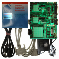
KIT DEVELOPMENT CAN MCP2510
Manufacturer
Microchip Technology
Specifications of DV251001
Main Purpose
Interface, CAN Controller
Embedded
Yes, MCU, 8-Bit
Utilized Ic / Part
MCP2510, MCP2515
Primary Attributes
Stand alone CAN Controller with SPI
Silicon Manufacturer
Microchip
Application Sub Type
CAN
Kit Application Type
Interface
Silicon Core Number
MCP2510, MCP2515
Kit Contents
Board Cable Power Supply CD
Lead Free Status / RoHS Status
Lead free / RoHS Compliant
Secondary Attributes
-
Lead Free Status / RoHS Status
na, Lead free / RoHS Compliant
Other names
DV251001R
DV251001R
DV251001R
Available stocks
Company
Part Number
Manufacturer
Quantity
Price
Company:

Part Number:
DV251001
Manufacturer:
MICROCHIP
Quantity:
12 000


SPI™ Compatible Serial EEPROM Family – Page Write mode, HOLD pin, software enabled block write protection and hardware write-protect pin. Supports SPI™ modes 0, 3. (continued)
25LC160A
25AA160A
25LC160B
25AA160B
25C320
25LC320
25AA320
25LC640
25AA640
Identification Products (Application-Specific Products for Monitors, DRAM Modules, ACR Risers and Other Plug-And-Play Applications)
24LC21
24LCS21
24LC21A
24LCS21A
24LCS22A
24LC024
24LC025
24AA52
24LCS52
NOTE:
NOTE:
Product
Product
Family Products
All 25-series products are available in Pb-free packages. Order with “G” suffix. Example: 25LC080AT-I/MSG. X/ST package code denotes rotated pinout.
Pb-free packages also available. Order with “G” suffix. Example: 24LCS52T-I/STG.
Memory
Cycles
Cycles
100K
E/W
E/W
1M
1M
1M
1M
1M
1M
1M
1M
1M
1M
1M
1M
1M
1M
1M
1M
1M
(Organization)
(Organization)
16 Kbits (x8)
16 Kbits (x8)
16 Kbits (x8)
16 Kbits (x8)
32 Kbits (x8)
32 Kbits (x8)
32 Kbits (x8)
64 Kbits (x8)
64 Kbits (x8)
1 Kbits (x8)
1 Kbits (x8)
1 Kbits (x8)
1 Kbits (x8)
2 Kbits (x8)
2 Kbits (x8)
2 Kbits (x8)
2 Kbits (x8)
2 Kbits (x8)
Density
Density
Write Speed
Page Size
10 ms
10 ms
10 ms
10 ms
10 ms
10 ms
10 ms
10 ms
10 ms
32B
32B
32B
16B
16B
32B
32B
32B
32B
Write Speed
Max. Clock
Frequency
400 kHz
400 kHz
400 kHz
400 kHz
400 kHz
400 kHz
400 kHz
400 kHz
400 kHz
5 ms
5 ms
5 ms
5 ms
5 ms
5 ms
5 ms
5 ms
5 ms
Operating Voltage (V)
Max. Clock
Frequency
10 MHz
10 MHz
10 MHz
10 MHz
3 MHz
2 MHz
1 MHz
3 MHz
1 MHz
2.5 to 5.5
2.5 to 5.5
2.5 to 5.5
2.5 to 5.5
2.5 to 5.5
2.5 to 5.5
2.5 to 5.5
1.8 to 5.5
2.5 to 5.5
Operating Voltage
2.5 to 5.5
1.8 to 5.5
2.5 to 5.5
1.8 to 5.5
4.5 to 5.5
2.5 to 5.5
1.8 to 5.5
2.5 to 5.5
1.8 to 5.5
(V)
Temps
C, I
C, I
C, I
C, I
C, I
C, I
I
I
I
Temps
I, E
I, E
I, E
I, E
I, E
I
I
I
I
Completely implements DDC1™/DDC2™ interface for VESA
monitor identification. Improved noise filter. Write protection
pin. Not recommended for new designs. Use 24LC21A or
24LCS21A.
Same as 24LC21 plus software enabled write-protect pin. Not
recommended for new designs. Use 24LC21A or 24LCS21A. P, SN
Same as 24LC21 plus “return to DDC1” feature.
Same as 24LC21A plus software enabled write-protect pin.
Implements VESA E-EDID 1.3 for flat panels and projectors.
Includes “return to DDC1” feature and software - enabled write
protect pin.
Addressable, hardware write protection for DRAM DIMM
modules and other applications.
Addressable. No write-protect.
Addressable, hardware write protection and software write
protection for lower half of the array. Designed for DRAM
DIMM modules.
Unique Features
Unique Features
P, SN, ST, MS
P, SN, ST, MS
P, SN, ST, MS
P, SN, ST, MS
P, SN
P, SN, X/ST
P, SN, X/ST
P, SN, X/ST
P, SN, X/ST
P, SN
P, SN
P, SN
P, SN
P, SN, ST, MS
P, SN, ST, MS
P, SN, ST, MS
P, SN, ST, MS
Packages
Packages
(Note)
(Note)
PAGE 49
Related parts for DV251001
Image
Part Number
Description
Manufacturer
Datasheet
Request
R

Part Number:
Description:
Manufacturer:
Microchip Technology Inc.
Datasheet:
Part Number:
Description:
Manufacturer:
Microchip Technology Inc.
Datasheet:
Part Number:
Description:
Manufacturer:
Microchip Technology Inc.
Datasheet:
Part Number:
Description:
Manufacturer:
Microchip Technology Inc.
Datasheet:
Part Number:
Description:
Manufacturer:
Microchip Technology Inc.
Datasheet:
Part Number:
Description:
Manufacturer:
Microchip Technology Inc.
Datasheet:
Part Number:
Description:
Manufacturer:
Microchip Technology Inc.
Datasheet:
Part Number:
Description:
Manufacturer:
Microchip Technology Inc.
Datasheet: