EVL6563S-100W STMicroelectronics, EVL6563S-100W Datasheet - Page 29
EVL6563S-100W
Manufacturer Part Number
EVL6563S-100W
Description
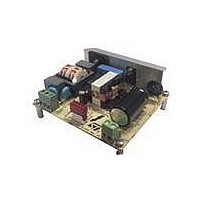
EVAL BOARD FOR L6563(100W)
Manufacturer
STMicroelectronics
Type
Power Factor Correctionr
Specifications of EVL6563S-100W
Main Purpose
Power Management, Power Factor Correction
Embedded
No
Utilized Ic / Part
L6563
Primary Attributes
100W Power Factor Correction and Preregulator Combination
Secondary Attributes
Transition Mode & Active Tracking Boost Function.
Board Size
90 mm x 83 mm
Maximum Operating Temperature
+ 60 C
Operating Supply Voltage
90 V to 265 V
Product
Power Management Modules
Dimensions
90 mm x 83 mm
Lead Free Status / RoHS Status
Lead free / RoHS Compliant
For Use With/related Products
L6563S
Other names
497-10490


L6563S
V(TBO)/RT, that is internally 1:1 mirrored and sunk from pin INV (#1) input of the L6563S's
error amplifier. In this way, when the mains voltage increases the voltage at TBO pin will
increase as well and so will do the current flowing through the resistor connected between
TBO and GND. Then a larger current will be sunk by INV pin and the output voltage of the
PFC pre-regulator will be forced to get higher. Obviously, the output voltage will move in the
opposite direction if the input voltage decreases.
To avoid undesired output voltage rise should the mains voltage exceed the maximum
specified value, the voltage at the TBO pin is clamped at 3V. By properly selecting the
multiplier bias it is possible to set the maximum input voltage above which input-to-output
tracking ends and the output voltage becomes constant. If this function is not used, leave
the pin open: the device will regulate a fixed output voltage.
Starting from the following data:
●
●
●
●
●
to set the output voltage at the desired values use the following design procedure:
1.
2.
3.
4.
5.
Figure 40
Vin
Vin
Vo
Vo
Vox = absolute maximum limit for the regulated output voltage;
Determine the input RMS voltage Vinclamp that produces Vo = Vox:
and choose a value Vin
of the output voltage range below Vox (it will equal Vox if one chooses Vin
Determine the divider ratio of the MULT pin (#3) bias:
and check that at minimum mains voltage Vin1 the peak voltage on pin 3 is greater than
0.65 V.
Determine R1, the upper resistor of the output divider, for instance 3 MΩ.
Calculate the lower resistor R2 of the output divider and the adjustment resistor RT:
Check that the maximum current sourced by the TBO pin (#6) does not exceed the
maximum specified (0.2 mA):
1
2
1
2
= regulated output voltage @ Vin = Vin
= regulated output voltage @ Vin = Vin
= minimum specified input RMS voltage;
= maximum specified input RMS voltage;
shows the internal block diagram of the tracking boost function.
⎧
⎪ ⎪
⎨
⎪
⎪
⎩
R
R
Vin
2
T
=
=
clamp
2
x
5 .
2
such that Vin
Doc ID 16116 Rev 4
⋅
⋅
=
R
k
1
⋅
I
Vox
Vo
TBO
R
⋅
(
1
Vo
2
⋅
max
Vin
−
−
Vo
1
k
Vo
Vo
−
=
2
2
=
2
2
1
1
−
−
5 .
R
≤
3
⋅
2
Vin
Vo
T
)
Vin
Vinx < Vinclamp. This will result in a limitation
⋅
⋅
3
Vin
≤
Vin
Vin
1
1
2
1
2
;
;
0
2 .
−
2
x
2
−
Vox
−
Vo
⋅
10
(
Vin
Vo
2
−
−
3
−
1
2
Vo
Vo
−
2
2
1
5 .
⋅
)
Vin
⋅
Vin
Application information
1
1
x
= Vin
clamp
29/43
)
Related parts for EVL6563S-100W
Image
Part Number
Description
Manufacturer
Datasheet
Request
R

Part Number:
Description:
EVAL BOARD FOR L6563(250W)
Manufacturer:
STMicroelectronics
Datasheet:

Part Number:
Description:
EVAL BOARD FOR L6563(400W)
Manufacturer:
STMicroelectronics
Datasheet:

Part Number:
Description:
Power Management Modules & Development Tools Tranisition Mode PFC L6563S EVL Board
Manufacturer:
STMicroelectronics
Datasheet:

Part Number:
Description:
EVAL BOARD L6563 (200W)
Manufacturer:
STMicroelectronics
Datasheet:
Part Number:
Description:
STMicroelectronics [RIPPLE-CARRY BINARY COUNTER/DIVIDERS]
Manufacturer:
STMicroelectronics
Datasheet:
Part Number:
Description:
STMicroelectronics [LIQUID-CRYSTAL DISPLAY DRIVERS]
Manufacturer:
STMicroelectronics
Datasheet:

Part Number:
Description:
BOARD EVAL FOR MEMS SENSORS
Manufacturer:
STMicroelectronics
Datasheet:
Part Number:
Description:
NPN TRANSISTOR POWER MODULE
Manufacturer:
STMicroelectronics
Datasheet:
Part Number:
Description:
TURBOSWITCH ULTRA-FAST HIGH VOLTAGE DIODE
Manufacturer:
STMicroelectronics
Datasheet:
Part Number:
Description:
Manufacturer:
STMicroelectronics
Datasheet:
Part Number:
Description:
DIODE / SCR MODULE
Manufacturer:
STMicroelectronics
Datasheet:
Part Number:
Description:
DIODE / SCR MODULE
Manufacturer:
STMicroelectronics
Datasheet: