NBC124XXEVB ON Semiconductor, NBC124XXEVB Datasheet - Page 10
NBC124XXEVB
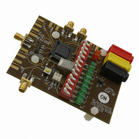
Manufacturer Part Number
NBC124XXEVB
Description
EVAL BOARD FOR NBC124XX
Manufacturer
ON Semiconductor
Datasheets
1.NBC12439FAR2G.pdf
(21 pages)
2.NBC12429FAR2G.pdf
(22 pages)
3.NBC12430FAR2G.pdf
(20 pages)
Specifications of NBC124XXEVB
Design Resources
NBC124XXEVB Gerber Files
Main Purpose
Timing, PLL
Embedded
No
Utilized Ic / Part
NBC12429, NBC12430, NBC12439
Primary Attributes
DIP Switch Controlled M & N Logic
Secondary Attributes
Push Button or Externally Controlled P_Load
Technology Type
Evaluation Board
Lead Free Status / RoHS Status
Lead free / RoHS Compliant
For Use With/related Products
NBC124XX
Other names
NBC124XXEVBOS


S_CLOCK signal samples the information on the S_DATA
line and loads it into a 14 bit shift register. Note that the
P_LOAD signal must be HIGH for the serial load operation
to function. The Test register is loaded with the first three
bits, the N register with the next two, and the M register with
the final nine bits of the data stream on the S_DATA input.
For each register, the most significant bit is loaded first (T2,
N1, and M8). A pulse on the S_LOAD pin after the shift
register is fully loaded will transfer the divide values into the
counters. The HIGH to LOW transition on the S_LOAD
input will latch the new divide values into the counters.
Figures 5 and 6 illustrate the timing diagram for both a
parallel and a serial load of the device synthesizer.
powerup through the parallel interface, and then possibly
M[8:0] and N[1:0] are normally specified once at
http://onsemi.com
10
again through the serial interface. This approach allows the
application to come up at one frequency and then change or
fine−tune the clock as the ability to control the serial
interface becomes available.
internal nodes as determined by the T[2:0] bits in the serial
configuration stream. It is not configurable through the
parallel interface. The T2, T1, and T0 control bits are preset
to ‘000’ when P_LOAD is LOW so that the PECL F
outputs are as jitter−free as possible. Any active signal on the
TEST output pin will have detrimental affects on the jitter
of the PECL output pair. In normal operations, jitter
specifications are only guaranteed if the TEST output is
static. The serial configuration port can be used to select one
of the alternate functions for this pin.
The TEST output provides visibility for one of the several
OUT
Related parts for NBC124XXEVB
Image
Part Number
Description
Manufacturer
Datasheet
Request
R

Part Number:
Description:
ON Semiconductor [VOLTAGE REGULATOR]
Manufacturer:
ON Semiconductor
Datasheet:
Part Number:
Description:
357-036-542-201 CARDEDGE 36POS DL .156 BLK LOPRO
Manufacturer:
ON Semiconductor
Datasheet:
Part Number:
Description:
357-036-542-201 CARDEDGE 36POS DL .156 BLK LOPRO
Manufacturer:
ON Semiconductor
Datasheet:
Part Number:
Description:
357-036-542-201 CARDEDGE 36POS DL .156 BLK LOPRO
Manufacturer:
ON Semiconductor
Datasheet:
Part Number:
Description:
357-036-542-201 CARDEDGE 36POS DL .156 BLK LOPRO
Manufacturer:
ON Semiconductor
Datasheet:
Part Number:
Description:
357-036-542-201 CARDEDGE 36POS DL .156 BLK LOPRO
Manufacturer:
ON Semiconductor
Datasheet:
Part Number:
Description:
357-036-542-201 CARDEDGE 36POS DL .156 BLK LOPRO
Manufacturer:
ON Semiconductor
Datasheet:
Part Number:
Description:
357-036-542-201 CARDEDGE 36POS DL .156 BLK LOPRO
Manufacturer:
ON Semiconductor
Datasheet:
Part Number:
Description:
357-036-542-201 CARDEDGE 36POS DL .156 BLK LOPRO
Manufacturer:
ON Semiconductor
Datasheet:
Part Number:
Description:
357-036-542-201 CARDEDGE 36POS DL .156 BLK LOPRO
Manufacturer:
ON Semiconductor
Datasheet:
Part Number:
Description:
357-036-542-201 CARDEDGE 36POS DL .156 BLK LOPRO
Manufacturer:
ON Semiconductor
Datasheet:
Part Number:
Description:
Manufacturer:
ON Semiconductor
Datasheet:
Part Number:
Description:
Manufacturer:
ON Semiconductor
Datasheet:
Part Number:
Description:
Manufacturer:
ON Semiconductor
Datasheet: