MCP4XXXDM-DB Microchip Technology, MCP4XXXDM-DB Datasheet
MCP4XXXDM-DB
Specifications of MCP4XXXDM-DB
Available stocks


Related parts for MCP4XXXDM-DB

MCP4XXXDM-DB Summary of contents
Page 1
... MCP4XXX Digital Potentiometer © 2006 Microchip Technology Inc. Daughter Board User’s Guide DS51621A ...
Page 2
... Select Mode, Smart Serial, SmartTel, Total Endurance, UNI/O, WiperLock and ZENA are trademarks of Microchip Technology Incorporated in the U.S.A. and other countries. SQTP is a service mark of Microchip Technology Incorporated in the U.S.A. All other trademarks mentioned herein are property of their respective companies. ...
Page 3
... A.6 Bottom Layer A.7 Top Components And Silk Screen Appendix B. Bill Of Materials (BOM) .......................................................................... 29 Appendix C. Board Testing ......................................................................................... 31 C.1 What is Tested ............................................................................................. 32 C.2 What is NOT Tested .................................................................................... 32 Worldwide Sales and Service ..................................................................................... 34 © 2005 Microchip Technology Inc. DAUGHTER BOARD USER’S GUIDE Table of Contents ....................................................................... 25 ................................................................................................. 26 ............................................................................................ 27 ........................................................... 28 ...
Page 4
... MCP4XXX Digital Potentiometer Daughter Board User’s Guide NOTES: DS51621A-page iv © 2005 Microchip Technology Inc. ...
Page 5
... Appendix A. “Schematics and Layouts” – Shows the schematic and layout diagrams for the MCP4XXX Digital Potentiometer Daughter Board. • Appendix B. “Bill Of Materials (BOM)” – Lists the parts used to build the MCP4XXX Digital Potentiometer Daughter Board. © 2006 Microchip Technology Inc. DAUGHTER BOARD USER’S GUIDE Preface NOTICE TO CUSTOMERS ® ...
Page 6
... DS21978 MCP41010 DS21978 MCP41050 DS21978 MCP41100 DS21978 MCP42010 DS21945 MCP42050 DS21945 MCP42100 DS21945 — DS21945 — Examples ® MPLAB IDE User’s Guide ...is the only compiler... Device Literature # DS11195 DS11195 DS11195 DS11195 DS11195 DS11195 — — © 2006 Microchip Technology Inc. ...
Page 7
... Local sales offices are also available to help customers. A listing of sales offices and locations is included in the back of this document. Technical support is available through the web site at: http://support.microchip.com. DOCUMENT REVISION HISTORY Revision A (July 2006) • Initial Release of this Document. © 2006 Microchip Technology Inc. DS51621A-page 3 ...
Page 8
... MCP4XXX Digital Potentiometer Daughter Board User’s Guide NOTES: DS51621A-page 4 © 2006 Microchip Technology Inc. ...
Page 9
... WHAT IS THE MCP4XXX DIGITAL POTENTIOMETER DAUGHTER BOARD? The MCP4XXX Digital Potentiometer Daughter Board allows the system designer to quickly evaluate the operation of Microchip Technology’s MCP42XXX and MCP4021 Digital Potentiometers. The MCP42XXX are dual Digital Potentiometer devices that have the same characteristics as their single Digital Potentiometer devices (MCP41XXX) ...
Page 10
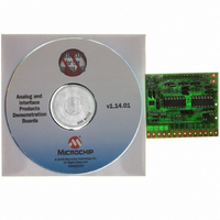
... WHAT THE MCP4XXX DIGITAL POTENTIOMETER DAUGHTER BOARD KIT INCLUDES This MCP4XXX Digital Potentiometer Daughter Board Kit includes: • MCP4XXX Digital Potentiometer Daughter Board • Analog and Interface Products Demonstration Boards CD-ROM (DS21912) - MCP4XXX Digital Potentiometer Daughter Board User’s Guide DS51621A-page 6 © 2006 Microchip Technology Inc. ...
Page 11
... Pads for easy connection to the Digital Potentiometer signals, including the Resistor Network Terminals and the Serial Interface signals • Connection terminals may be either through-hole or surface-mount © 2006 Microchip Technology Inc. DAUGHTER BOARD USER’S GUIDE voltage for WiperLock™ Technology ...
Page 12
... These footprints are provided so the customer can populate with the desired resistor value or leave unpopulated (open). FIGURE 2-1: Network Circuit Configuration. DS51621A-page 8 NOTE U2-P1A U2-P1W U2-P1B U1-P0A U1-P0W U1-P0B NOTE U2-P0A U2-P0W U2-P0B NOTE U1-P1W MCP4XXX Digital Potentiometer Daughter Board Resistor NOTE U3-A U3-W U3-B © 2006 Microchip Technology Inc. ...
Page 13
... FIGURE 2-2: © 2006 Microchip Technology Inc. MCP4XXX Digital Potentiometer Daughter Board Circuit. DS51621A-page 9 ...
Page 14
... There are sixteen connection points/pads that can use either through-hole or surface-mount connector posts and two through hole connections for power/ground. The connections to the SPI signals can be via the center taps of the JMP2 (SCK/SCL), JMP3 (SDO), and JMP4 (SDI/SDA) jumpers. DS51621A-page 10 © 2006 Microchip Technology Inc. ...
Page 15
... Using PICDEM HPC Board (RC3) Using PICDEM FS USB Board (RB1) FIGURE 2-3: Jumper JMP2, JMP3, and JMP4 Configurations. © 2006 Microchip Technology Inc. JMP2 - SPI Data Out Destination Using PICDEM HPC Board (RC4) Using PICDEM FS USB Board (RB0) JMP4 - SPI Data In Source ...
Page 16
... H.V. Commands) PICDEM Header - H3 (RC1) FIGURE 2-4: Jumper JMP1, JMP5, and JMP6 Configurations. DS51621A-page 12 JMP1 - CS0 Destination JMP6 selection connects to U3 JMP6 selection connects to U1 JMP5 - CS1 Source TC1240A VOUT (for H.V. Commands) PICDEM Header - H3 (RE2) © 2006 Microchip Technology Inc. ...
Page 17
... U3-B → U1-P0B (typically device removed for this configuration) FIGURE 2-5: Jumper JP7, JP9, JP10, JP11, JP12, and JP13 Configurations. © 2006 Microchip Technology Inc. JP7 JMP4 SDO selection is connected to U2-SI pin and U1-SO signal goes to U5-1 (input to 2-input OR gate) U1 Serial Out (SO) ...
Page 18
... Jumper JP1, JP2, JP3, JP4, JP5, and JP6 Configurations. DS51621A-page 14 JP1, JP2, JP4 JP4 - U2-P0A is floating (or pulled to VDD via R3) JP2 - U2-P0B is floating (or pulled to VSS via R1) JP1 - U2-P0W not connected to U2-P0B JP4 - U2-P0A is connected to VDD JP2 - U2-P0B is connected to VSS JP1 - U2-P0W is connected to U2-P0B © 2006 Microchip Technology Inc. ...
Page 19
... TABLE 2-1: Device R2, R3, R5, R7, R9, R10, R13, R15, R16 R1, R4, R11, R12, R14 R20, R21 © 2006 Microchip Technology Inc. OPTIONAL PASSIVE COMPONENTS Comment Pull-up resistor Pull-down resistor In-line resistor. Connected between the U1 wiper outputs and the PICDEM 28-pin header (H3) A/D pins. This is default open due to the PICDEM Demo Boards may have circuitry on these pins which would effect the wiper operation ...
Page 20
... Socket U1 Socket U1 Socket U2 Socket U2 Socket U3 Jumpers Device Configuration Required U2-Pot0 is windowed U2-Pot1 is windowed U1-Pot0 is windowed U2-Rheo0 Trims R1 U2-Rheo1 Trims R16 U1-Pot0 is windowed ) and ground (V ), which DD SS Potentiometer 0 Potentiometer 1 Potentiometer 0 Potentiometer 1 Device only contains single Potentiometer Comments © 2006 Microchip Technology Inc. ...
Page 21
... U2-Pot0 and U2-Pot1 to mid-scale. The Wiper (U1-P0W) is loaded with values to create a Triangle waveform. U1-Pot1 is connected to Power and Ground, and the Wiper (U1-P1W) is loaded with values to create an inverse Triangle waveform Channel 3 U2-P0A U2-P0W U2-P0B FIGURE 2-7: © 2006 Microchip Technology Inc. U2-P1A U2-P1W U2-P1B U1-P0A U1-P0W U1-P0B V B U1-P1A ...
Page 22
... MCP4XXX Digital Potentiometer Daughter Board User’s Guide Channel 4 Channel 2 Channel 1 Channel 3 FIGURE 2-8: Demo Jumper Configuration for use with PICDEM HPC Explorer Demo Board. DS51621A-page 18 © 2006 Microchip Technology Inc. ...
Page 23
... Channel 4 Channel 2 Channel 1 Channel 3 FIGURE 2-9: Demo Jumper Configuration for use with PICDEM FS USB Demo Board. © 2006 Microchip Technology Inc. DS51621A-page 19 ...
Page 24
... MCP4XXX Digital Potentiometer Daughter Board User’s Guide FIGURE 2-10: DS51621A-page 20 Screen Capture of P0W and P1W Output Waveforms. © 2006 Microchip Technology Inc. ...
Page 25
... For information on how to use MPLAB-IDE, ICD 2, or any other aspect of the PICmicro Development tool platform, please refer to the appropriate documentation. Table 2-2 shows the sequence of steps to demonstrate the MCP4XXXDM-DB board (as shipped) with the PICDEM HPC Explorer Demo Board. TABLE 2-2: Step Action ...
Page 26
... For information on how to use MPLAB-IDE, ICD 2, or any other aspect of the PICmicro Development tool platform, please refer to the appropriate documentation. Table 2-3 shows the sequence of steps to demonstrate the MCP4XXXDM-DB board (as shipped) with the PICDEM FS USB Demo Board. TABLE 2-3: Step Action ...
Page 27
... Figure A.3 shows the schematic of the MCP4XXX Digital Potentiometer Daughter Board. Figure A.4 shows the layout for the top layer of the MCP4XXX Digital Potentiometer Daughter Board. The layer order is shown in Figure A-1. FIGURE A-1: © 2006 Microchip Technology Inc. DAUGHTER BOARD USER’S GUIDE LAYER ORDER Top Layer Bottom Layer ...
Page 28
... MCP4XXX Digital Potentiometer Daughter Board User’s Guide A.3 BOARD SCHEMATIC - DIGITAL CIRCUITRY DS51621A-page 24 © 2006 Microchip Technology Inc. ...
Page 29
... A.4 TOP LAYER AND SILK SCREEN © 2006 Microchip Technology Inc. DS51621A-page 25 ...
Page 30
... MCP4XXX Digital Potentiometer Daughter Board User’s Guide A.5 TOP LAYER DS51621A-page 26 © 2006 Microchip Technology Inc. ...
Page 31
... A.6 BOTTOM LAYER © 2006 Microchip Technology Inc. DS51621A-page 27 ...
Page 32
... MCP4XXX Digital Potentiometer Daughter Board User’s Guide A.7 TOP COMPONENTS AND SILK SCREEN DS51621A-page 28 © 2006 Microchip Technology Inc. ...
Page 33
... Shunts Shunt,SHORT BLKS W TAB BLK Note 1: The components listed in this Bill of Materials are representative of the PCB assembly. The released BOM used in manufacturing uses all RoHS-compliant components. © 2006 Microchip Technology Inc. DAUGHTER BOARD USER’S GUIDE Description Technology Inc. Technology Inc. ...
Page 34
... R4 resistor on the PICDEM HPC Explorer Board (Rev 4 PCB) so that the circuitry on the AN1 signal line does not interfere with the operation of the U1-P0W signal. DS51621A-page 30 Description Manufacturer (1) Part Number — — — — © 2006 Microchip Technology Inc. ...
Page 35
... Figure C-1. The tested nodes are Channel 1 through Channel 4. Other configurations, Pad connections, and circuit performance are not tested. Channel 4 Channel 2 Channel 1 Channel 3 FIGURE C-1: Tested Jumper Configuration. © 2006 Microchip Technology Inc. DAUGHTER BOARD USER’S GUIDE DS51621A-page 31 ...
Page 36
... RA2 (P1W), RC2 (U/D), RC7 (SDO), RB5 (SHDN), RB4 (SHDN1), RB3 (SHDN0), RB1 (SCK/SCL), and RB0 (SDI/SDA) • Pads: U3UD, U3A, U3W, U3B, U1CS0 (U3CS), U2CS1, U2P1W, U2P1A, U2P0A, and U2P0B • Connections to unpopulated components DS51621A-page 32 © 2006 Microchip Technology Inc. ...
Page 37
... NOTES: © 2006 Microchip Technology Inc. DS51621A-page 33 ...
Page 38
... Fax: 886-3-572-6459 Taiwan - Kaohsiung Tel: 886-7-536-4818 Fax: 886-7-536-4803 Taiwan - Taipei Tel: 886-2-2500-6610 Fax: 886-2-2508-0102 Thailand - Bangkok Tel: 66-2-694-1351 Fax: 66-2-694-1350 © 2006 Microchip Technology Inc. EUROPE Austria - Wels Tel: 43-7242-2244-3910 Fax: 43-7242-2244-393 Denmark - Copenhagen Tel: 45-4450-2828 Fax: 45-4485-2829 France - Paris Tel: 33-1-69-53-63-20 ...