MCP3421DM-BFG Microchip Technology, MCP3421DM-BFG Datasheet - Page 14
MCP3421DM-BFG
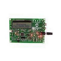
Manufacturer Part Number
MCP3421DM-BFG
Description
BOARD DEMO FOR MCP3421
Manufacturer
Microchip Technology
Datasheets
1.MCP3421A2T-ECH.pdf
(42 pages)
2.MCP3421DM-BFG.pdf
(26 pages)
3.MCP3421A0T-ECH.pdf
(30 pages)
Specifications of MCP3421DM-BFG
Main Purpose
Power Management, Battery Gauge
Utilized Ic / Part
MCP3421
Processor To Be Evaluated
MCP3421
Lead Free Status / RoHS Status
Lead free / RoHS Compliant
Secondary Attributes
-
Embedded
-
Primary Attributes
-
Lead Free Status / RoHS Status
Lead free / RoHS Compliant, Lead free / RoHS Compliant


MCP3421
4.9.2
When the user gets the digital output codes from the
device as described in Section 4.9.1 “Digital output
code from device”, the next step is converting the
digital output codes to a measured input voltage.
Equation 4-4
output codes to its corresponding input voltage.
If the sign indicator bit (MSB) is ‘0’, the input voltage
is obtained by multiplying the output code with the LSB
and divided by the PGA setting.
If the sign indicator bit (MSB) is ‘1’, the output code
needs to be converted to two’s complement before
multiplied by LSB and divided by the PGA setting.
Table 4-4
output codes to input voltage.
TABLE 4-4:
DS22003E-page 14
[V
IN
Input Voltage
V
+ - V
REF
≤ -V
≥ V
-1 LSB
-2 LSB
- V
2 LSB
1 LSB
IN
- 1 LSB
shows an example of converting the device
0
REF
REF
-]
REF
CONVERTING THE DEVICE
OUTPUT CODE TO INPUT SIGNAL
VOLTAGE
•
shows an example of converting the
PGA]
EXAMPLE OF CONVERTING OUTPUT CODE TO VOLTAGE (WITH 18 BIT SETTING)
011111111111111111
011111111111111111
000000000000000010
000000000000000001
000000000000000000
111111111111111111
111111111111111110
100000000000000000
100000000000000000
Digital Output Code
(sign bit)
MSB
0
0
0
0
0
1
1
1
1
(2
2
(2
2
(0+0+0+0+0+0+0+0+0+0+0+0+0+0+0+2
LSB(15.625μV)/PGA = 31.25 (μV) for PGA = 1
(0+0+0+0+0+0+0+0+0+0+0+0+0+0+0+0+2
LSB(15.625μV)/PGA = 15.625 (μV)for PGA = 1
(0+0+0+0+0+0+0+0+0+0+0+0+0+0+0+0+0)x
LSB(15.625μV)/PGA = 0 V (V) for PGA = 1
-(0+0+0+0+0+0+0+0+0+0+0+0+0+0+0+0+2
LSB(15.625μV)/PGA = - 15.625 (μV)for PGA = 1
-(0+0+0+0+0+0+0+0+0+0+0+0+0+0+0+2
LSB(15.625μV)/PGA = - 31.25 (μV)for PGA = 1
-(2
LSB(15.625μV)/PGA = - 2.048 (V) for PGA = 1
-(2
LSB(15.625μV)/PGA = - 2.048 (V) for PGA = 1
Example of Converting Output Codes to Input Voltage
1
1
+2
+2
16
16
17
17
+2
+2
0
0
EQUATION 4-4:
)x LSB(15.625μV)/PGA = 2.048 (V) for PGA = 1
)x LSB(15.625μV)/PGA = 2.048 (V) for PGA = 1
+0+0+0+0+0+0+0+0+0+0+0+0+0+0+0+0+0) x
+0+0+0+0+0+0+0+0+0+0+0+0+0+0+0+0+0) x
Where:
15
15
If MSB = 0 (Positive Output Code):
If MSB = 1 (Negative Output Code):
2’s complement
+2
+2
Input Voltage
14
14
+2
+2
Input Voltage
13
13
+2
+2
LSB
12
12
=
+2
+2
(2
11
11
′
+2
+2
s complement of Output Code)
=
=
CONVERTING OUTPUT
CODES TO INPUT
VOLTAGE
=
10
10
© 2009 Microchip Technology Inc.
+2
+2
(Output Code)
See
1’s complement + 1
9
9
+2
+2
8
8
Table 4-1
+2
+2
1
7
7
+0)x
1
+2
+2
+0)x
0
)x
0
6
6
)x
+2
+2
•
----------- -
PGA
LSB
5
5
+2
+2
4
4
+2
+2
•
3
3
----------- -
PGA
+2
+2
LSB
2
2
+
+
Related parts for MCP3421DM-BFG
Image
Part Number
Description
Manufacturer
Datasheet
Request
R

Part Number:
Description:
18-Bit Analog-to-Digital Converter with I2C Interface and On-Board Reference
Manufacturer:
Microchip Technology
Datasheet:

Part Number:
Description:
Manufacturer:
Microchip Technology Inc.
Datasheet:
Part Number:
Description:
Manufacturer:
Microchip Technology Inc.
Datasheet:
Part Number:
Description:
Manufacturer:
Microchip Technology Inc.
Datasheet:
Part Number:
Description:
Manufacturer:
Microchip Technology Inc.
Datasheet:
Part Number:
Description:
Manufacturer:
Microchip Technology Inc.
Datasheet:
Part Number:
Description:
Manufacturer:
Microchip Technology Inc.
Datasheet:
Part Number:
Description:
Manufacturer:
Microchip Technology Inc.
Datasheet:
Part Number:
Description:
Manufacturer:
Microchip Technology Inc.
Datasheet: