MCP3909RD-3PH1 Microchip Technology, MCP3909RD-3PH1 Datasheet - Page 15
MCP3909RD-3PH1
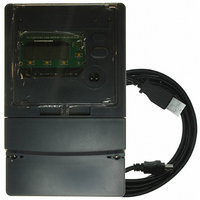
Manufacturer Part Number
MCP3909RD-3PH1
Description
REF DESIGN MCP3909 3PH ENGY MTR
Manufacturer
Microchip Technology
Datasheets
1.MCP3909T-ISS.pdf
(44 pages)
2.MCP3909T-ISS.pdf
(104 pages)
3.MCP3909RD-3PH3.pdf
(88 pages)
Specifications of MCP3909RD-3PH1
Main Purpose
Power Management, Energy/Power Meter
Embedded
No
Utilized Ic / Part
MCP3909, PIC18F2520, PIC18F4550
Primary Attributes
3-Ph, 220 VAC, In Case, LCD, USB, GUI
Secondary Attributes
Opto-Isolated Interface for Safety
Operating Voltage
220 V
Operating Current
5 A
Description/function
Energy Meter
For Use With/related Products
MCP3909
Lead Free Status / RoHS Status
Not applicable / Not applicable


3.0
The descriptions of the pins are listed in
TABLE 3-1:
3.1
DV
within the MCP3909.
This pin requires appropriate bypass capacitors and
should be maintained to 5V ±10% for specified
operation.
Information”.
3.2
HPF controls the state of the high-pass filter in both
input channels. A logic ‘1’ enables both filters,
removing any DC offset coming from the system or the
device. A logic ‘0’ disables both filters allowing DC
voltages to be measured.
© 2009 Microchip Technology Inc.
DD
MCP3909
is the power supply pin for the digital circuitry
SSOP
PIN DESCRIPTIONS
Digital V
High-Pass Filter Input Logic Pin
(HPF)
10
11
12
13
14
15
16
17
18
19
20
21
22
23
24
1
2
3
4
5
6
7
8
9
Refer
PIN FUNCTION TABLE
DD
to
(DV
REFIN/OUT
SDO / NEG
Section 6.0
SCK / F2
SDI / F1
Symbol
CS / F0
HF
MCLR
OSC1
OSC2
F
F
CH0+
CH1+
DV
A
D
AV
CH0-
CH1-
HPF
DD
OUT1
OUT0
NC
NC
G1
G0
GND
GND
OUT
DD
DD
)
“Applications
Table
Digital Power Supply Pin
High-Pass Filters Control Logic Pin
Analog Power Supply Pin
No Connect
Master Clear Logic Input Pin
Analog Ground Pin, Return Path for internal analog circuitry
Serial Clock or Frequency Control for HF
Serial Data Input or Frequency Control for F
Chip Select or Frequency Control for F
Gain Control Logic Input Pin
Gain Control Logic Input Pin
Oscillator Crystal Connection Pin or Clock Input Pin
Oscillator Crystal Connection Pin or Clock Output Pin
No Connect
Serial Data Out or Negative Power Logic Output Pin
Digital Ground Pin, Return Path for Internal Digital Circuitry
High-Frequency Logic Output Pin (Intended for Calibration)
Differential Mechanical Counter Logic Output Pin
Differential Mechanical Counter Logic Output Pin
Non-Inverting Analog Input Pin for Channel 0 (Current Channel)
Inverting Analog Input Pin for Channel 0 (Current Channel)
Inverting Analog Input Pin for Channel 1 (Voltage Channel)
Non-Inverting Analog Input Pin for Channel 1 (Voltage Channel)
Voltage Reference Input/Output Pin
3-1.
3.3
AV
within the MCP3909.
This pin requires appropriate bypass capacitors and
should be maintained to 5V ±10% for specified
operation.
Information”.
DD
is the power supply pin for the analog circuitry
Analog V
Description
Refer
OUT0/1
OUT
to
OUT0/1
DD
Logic Input Pin
Logic Input Pin
(AV
Section 6.0
Logic Input Pin
DD
MCP3909
)
DS22025B-page 15
“Applications
Related parts for MCP3909RD-3PH1
Image
Part Number
Description
Manufacturer
Datasheet
Request
R

Part Number:
Description:
BOARD DES MCP3909 ENERGY METER
Manufacturer:
Microchip Technology
Datasheet:

Part Number:
Description:
REF DESIGN FOR MCP3909 W/18F2520
Manufacturer:
Microchip Technology
Datasheet:

Part Number:
Description:
Manufacturer:
Microchip Technology Inc.
Datasheet:
Part Number:
Description:
Manufacturer:
Microchip Technology Inc.
Datasheet:
Part Number:
Description:
Manufacturer:
Microchip Technology Inc.
Datasheet:
Part Number:
Description:
Manufacturer:
Microchip Technology Inc.
Datasheet:
Part Number:
Description:
Manufacturer:
Microchip Technology Inc.
Datasheet:
Part Number:
Description:
Manufacturer:
Microchip Technology Inc.
Datasheet:
Part Number:
Description:
Manufacturer:
Microchip Technology Inc.
Datasheet:
Part Number:
Description:
Manufacturer:
Microchip Technology Inc.
Datasheet: