74LVC2G66EVB NXP Semiconductors, 74LVC2G66EVB Datasheet
74LVC2G66EVB
Specifications of 74LVC2G66EVB


Related parts for 74LVC2G66EVB


74LVC2G66EVB Summary of contents
Page 1
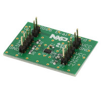
Demonstrate fast switching of HF signals with a dual SPST analog switch This compact demo board makes it easy to evaluate the 74LVC2G66, a dual SPST analog switch that supports high-frequency bandwidth and has control inputs tolerant to over-supply voltage. Key features and benefits } Wide supply voltage range (1.65 to 5.5 V) and low Ron (5 Ω typ) for design flexibility } High bandwidth (up to 500 MHz) for data-rich applications } High speed with lower propagation delay of 0.4 ns typ } Ability to monitor input and output rise/fall times, plus propagation delays with different loads (capacitors and resistors ver-supply voltage tolerance up to 5.5 V for enable inputs } Low ON state capacitance (9.5 pF typ) for better signal integrity } Fully specified for use in harsh conditions (- and -40 to 125 °C) } Excellent ESD performance (7.5 kV HBM), suitable for ...
Page 2
To turn a switch ON (close the contact), a logic HIGH signal needs to be connected to the respective Enable pin. To connect the Enable pins and GND leads of an oscilloscope probe to the board, additional connectors Circuit schematic of 74LVC2G66 demo board (JP1 and JP2) with VCC and GND pins are provided. Also, loads 500 Ω 4.7 kΩ and C2 = 5.6 pF are provided so designers can see variations in the output rise and fall times at resistive and capacitive loads. ...
Page 3
Test results Results of testing done on the 74LVC2G66 evaluation board are shown in the figures below. In Figure 1, the purple waveform is a 500 kHz square wave input with an amplitude applied at the 1Z pin, and the green waveform is the switch output at the 1Y pin with a load of 500 Ω when the Enable pin (1E) is pulled high and the switch is ON. The supply voltage V for the switch Figure 2, the green CC waveform shows the output at the 1Y pin when Enable pin (1E) is connected to GND and the switch is OFF. The supply voltage Figure 1 Figure 3 V for the switch is still 3 V, and the purple input signal at the CC 1Z pin Figure 3, the purple waveform shows a 5 MHz input signal the 1Z input, and the green waveform is the output of approx. 2. the 1Y output when the supply voltage VCC and the1E pin logic HIGH level Figure 4, the purple waveform input signal with a 5 MHz frequency at the1Z input of the switch, and the green waveform is an approx signal at the 1Y output when the and the 1E pin is pulled LOW to GND. CC Figure 2 Figure 4 ...
Page 4
Packages The 74LVC2G66 is available in leadless 8-pin XSON, XSONU, and XQFN packages and in standard 8-pin TSSOP and VSSOP packages. Package suffix DP SOT505-2 8-pin Width (mm) 3 Length (mm) 3 Height (mm) 1.1 Pitch (mm) 0.65 Ordering information Part number Temp. range 74LVC2G66DP -40 to 125 °C 74LVC2G66GD -40 to 125 °C 74LVC2G66DC -40 to 125 °C 74LVC2G66GT -40 to 125 °C 74LVC2G66GM -40 to 125 °C www.nxp.com © 2010 NXP B.V. All rights reserved. ...