74LVC2G66EVB NXP Semiconductors, 74LVC2G66EVB Datasheet - Page 3
74LVC2G66EVB
Manufacturer Part Number
74LVC2G66EVB
Description
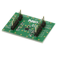
BOARD EVALUATION FOR 74LVC2G66
Manufacturer
NXP Semiconductors
Specifications of 74LVC2G66EVB
Main Purpose
Interface, Analog Switch
Embedded
No
Utilized Ic / Part
74LVC2G66
Primary Attributes
Dual SPST Analog Switch
Secondary Attributes
1.65 ~ 5.5 V Supply
Lead Free Status / RoHS Status
Lead free / RoHS Compliant
Other names
568-5081


Test results
Results of testing done on the 74LVC2G66 evaluation board
are shown in the figures below. In Figure 1, the purple
waveform is a 500 kHz square wave input with an amplitude
of 3 V applied at the 1Z pin, and the green waveform is the
switch output at the 1Y pin with a load of 500 Ω when the
Enable pin (1E) is pulled high to 3 V and the switch is ON. The
supply voltage V
waveform shows the output at the 1Y pin when Enable pin (1E)
is connected to GND and the switch is OFF. The supply voltage
Figure 1
Figure 3
CC
for the switch is 3 V. In Figure 2, the green
V
1Z pin is 3 V. In Figure 3, the purple waveform shows a 5 MHz
input signal of 3 V at the 1Z input, and the green waveform is
the output of approx. 2.84 V at the 1Y output when the supply
voltage VCC is 3 V and the1E pin is at a logic HIGH level of 3 V.
In Figure 4, the purple waveform is a 3 V input signal with a
5 MHz frequency at the1Z input of the switch, and the green
waveform is an approx. 97 mV signal at the 1Y output when the
V
Figure 2
Figure 4
CC
CC
for the switch is still 3 V, and the purple input signal at the
is 3 V and the 1E pin is pulled LOW to GND.
Related parts for 74LVC2G66EVB
Image
Part Number
Description
Manufacturer
Datasheet
Request
R

Part Number:
Description:
IC TRANSCVR TRI-ST DL 24SOIC
Manufacturer:
NXP Semiconductors
Datasheet:

Part Number:
Description:
IC ADDRESS/CLK DRIVER 56-TSSOP
Manufacturer:
IDT, Integrated Device Technology Inc
Datasheet:

Part Number:
Description:
IC MUX/DEMUX 2X1 6TSOP
Manufacturer:
NXP Semiconductors
Datasheet:

Part Number:
Description:
IC SWITCH QUAD SPST 14SOIC
Manufacturer:
NXP Semiconductors
Datasheet:

Part Number:
Description:
IC BUFF DVR TRI-ST 16BIT 48TSSOP
Manufacturer:
IDT, Integrated Device Technology Inc
Datasheet:

Part Number:
Description:
IC BUFF HEX OPEN DRAIN 14TSSOP
Manufacturer:
NXP Semiconductors
Datasheet:
Part Number:
Description:
IC BUFF HEX OPEN DRAIN 14SOICN
Manufacturer:
NXP Semiconductors
Datasheet:
Part Number:
Description:
IC BUFF DVR TRI-ST QD 14SSOP
Manufacturer:
NXP Semiconductors
Datasheet:
Part Number:
Description:
IC BUFF DVR TRI-ST QD 14SOICN
Manufacturer:
NXP Semiconductors
Datasheet:
Part Number:
Description:
IC BUFF DVR TRI-ST QD 14SOICN
Manufacturer:
NXP Semiconductors
Datasheet:
Part Number:
Description:
IC BUFF DVR TRI-ST QD 14SSOP
Manufacturer:
NXP Semiconductors
Datasheet:
Part Number:
Description:
IC BUFF DVR TRI-ST QD 14TSSOP
Manufacturer:
NXP Semiconductors
Datasheet:

Part Number:
Description:
IC BUFF/DVR TRI-ST DUAL 20SSOP
Manufacturer:
NXP Semiconductors
Datasheet:

Part Number:
Description:
IC BUFF/DVR TRI-ST DUAL 20SOIC
Manufacturer:
NXP Semiconductors
Datasheet:

Part Number:
Description:
IC BUFF/DVR TRI-ST DUAL 20TSSOP
Manufacturer:
NXP Semiconductors
Datasheet: