V2DIP2-64 FTDI, Future Technology Devices International Ltd, V2DIP2-64 Datasheet - Page 13
V2DIP2-64
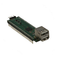
Manufacturer Part Number
V2DIP2-64
Description
MOD MCU-USB HOST CTLR 60-DIP
Manufacturer
FTDI, Future Technology Devices International Ltd
Series
Vinculum-IIr
Datasheet
1.V2DIP2-64.pdf
(24 pages)
Specifications of V2DIP2-64
Main Purpose
Interface, USB 2.0 Host/Controller
Embedded
Yes, ASIC
Utilized Ic / Part
VNC2-64Q
Primary Attributes
Dual A-Type Connector, UART / Parallel FIFO / SPI Interfaces
Secondary Attributes
LED Status Indicators
Lead Free Status / RoHS Status
Lead free / RoHS Compliant
Other names
768-1053


3.6 Parallel FIFO Interface-Asynchronous Mode
The Parallel FIFO Asynchronous mode is functionally the same as the Parallel FIFO Interface present in
VDIP2 has an eight bit data bus, individual read and write strobes and two hardware flow control signals.
3.6.1 Signal Description - Parallel FIFO Interface
The Parallel FIFO Interface signals can be programmed to a choice of available I/O pins.
shows the Parallel FIFO Interface signals and the pins that they can be mapped.
J2-18, J2-14, J1-17, J1-24, J1-29, J2-
28, J2-23, J1-3, J1-7, J2-8, J2-4
J2-17, J1-14, J1-18, J1-26, J1-30, J2-
27, J2-22, J1-4, J1-8, J2-7, J2-3
J2-16, J1-15, J1-20, J1-27, J2-30, J2-
26, J1-1, J1-5, J1-9, J2-6, J2-2
J2-15, JI-16, J1-21, J1-28, J2-29, J2-24,
J1-2, J1-6, J2-9, J2-5, J2-1
23, J1-3, J1-7, J2-8, J2-4
J2-17, J1-14, J1-18, J1-26, J1-30, J2-
27, J2-22, J1-4, J1-8, J2-7, J2-3
J2-16, J1-15, J1-20, J1-27, J2-30, J2-
26, J1-1, J1-5, J1-9, J2-6, J2-2
J2-15, JI-16, J1-21, J1-28, J2-29, J2-24,
J1-2, J1-6, J2-9, J2-5, J2-1
23, J1-3, J1-7, J2-8, J2-4
J2-17, J1-14, J1-18, J1-26, J1-30, J2-
27, J2-22, J1-4, J1-8, J2-7, J2-3
J2-16, J1-15, J1-20, J1-27, J2-30, J2-
26, J1-1, J1-5, J1-9, J2-6, J2-2
J2-15, JI-16, J1-21, J1-28, J2-29, J2-24,
J1-2, J1-6, J2-9, J2-5, J2-1
Table 3.6 - Data and Control Bus Signal Mode Options – Parallel FIFO Interface
J2-14, J1-17, J1-24, J1-29, J2-28, J2-
J2-14, J1-17, J1-24, J1-29, J2-28, J2-
Available Pins
Copyright © 2010 Future Technology Devices International Limited
`
fifo_data[0]
fifo_data[1]
fifo_data[2]
fifo_data[3]
fifo_data[4]
fifo_data[5]
fifo_data[6]
fifo_data[7]
V2DIP2-64 VNCL2-64Q Development Module Datasheet Version 1.01
fifo_txe#
fifo_rxf#
fifo_wr#
fifo_rd#
Name
Output
Output
Type
Input
Input
I/O
I/O
I/O
I/O
I/O
I/O
I/O
I/O
When high, do not read data
from the FIFO. When low, there
is data available in the FIFO
which can be read by strobing
RD# low, then high.
When high, do not write data into
the FIFO. When low, data can be
written into the FIFO by strobing
fifo_wr# high, then low.
Enables the current FIFO data
byte on D0...D7 when low.
Fetches the next FIFO data byte
(if available) from the receive
FIFO buffer when fifo_rd# goes
from high to low
Writes the data byte on the
D0...D7 pins into the transmit
FIFO buffer when fifo_wr# goes
from high to low.
Document Reference No.: FT_000166
FIFO data bus Bit 0
FIFO data bus Bit 1
FIFO data bus Bit 2
FIFO data bus Bit 3
FIFO data bus Bit 4
FIFO data bus Bit 5
FIFO data bus Bit 6
FIFO data bus Bit 7
Description
Clearance No.: FTDI# 155
Table 3.6
12
Related parts for V2DIP2-64
Image
Part Number
Description
Manufacturer
Datasheet
Request
R

Part Number:
Description:
MOD MCU-USB HOST CTLR 24-DIP
Manufacturer:
FTDI, Future Technology Devices International Ltd
Datasheet:

Part Number:
Description:
MOD MCU-USB HOST CTLR 40-DIP
Manufacturer:
FTDI, Future Technology Devices International Ltd
Datasheet:

Part Number:
Description:
IC USB TO SERIAL UART 32-QFN
Manufacturer:
FTDI, Future Technology Devices International Ltd

Part Number:
Description:
IC USB HOST CTLR VINCULUM 48LQFP
Manufacturer:
FTDI, Future Technology Devices International Ltd
Datasheet:

Part Number:
Description:
IC USB HOST VINCULUM-II 32QFN
Manufacturer:
FTDI, Future Technology Devices International Ltd
Datasheet:
Part Number:
Description:
IC USB HOST VINCULUM-II 32LQFN
Manufacturer:
FTDI, Future Technology Devices International Ltd
Datasheet:
Part Number:
Description:
IC USB HOST VINCULUM-II 48QFN
Manufacturer:
FTDI, Future Technology Devices International Ltd
Datasheet:
Part Number:
Description:
IC USB HOST VINCULUM-II 32LQFN
Manufacturer:
FTDI, Future Technology Devices International Ltd
Datasheet:
Part Number:
Description:
IC USB HOST VINCULUM-II 32QFN
Manufacturer:
FTDI, Future Technology Devices International Ltd
Datasheet:
Part Number:
Description:
IC USB HOST VINCULUM-II 48LQFP
Manufacturer:
FTDI, Future Technology Devices International Ltd
Datasheet:
Part Number:
Description:
IC USB HOST VINCULUM-II 48LQFP
Manufacturer:
FTDI, Future Technology Devices International Ltd
Datasheet:
Part Number:
Description:
IC USB HOST VINCULUM-II 48QFN
Manufacturer:
FTDI, Future Technology Devices International Ltd
Datasheet:
Part Number:
Description:
IC USB HOST CTLR VINCULUM 64QFN
Manufacturer:
FTDI, Future Technology Devices International Ltd
Datasheet:

Part Number:
Description:
IC USB HOST CTLR VINCULUM 64LQFP
Manufacturer:
FTDI, Future Technology Devices International Ltd
Datasheet:
Part Number:
Description:
IC USB HOST VINCULUM-II 64LQFP
Manufacturer:
FTDI, Future Technology Devices International Ltd
Datasheet: