AD5171EVAL Analog Devices Inc, AD5171EVAL Datasheet - Page 15
AD5171EVAL
Manufacturer Part Number
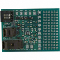
AD5171EVAL
Description
BOARD EVAL FOR AD5171
Manufacturer
Analog Devices Inc
Datasheet
1.AD5171BRJZ10-R7.pdf
(24 pages)
Specifications of AD5171EVAL
Main Purpose
Digital Potentiometer
Utilized Ic / Part
AD5171
Lead Free Status / RoHS Status
Contains lead / RoHS non-compliant
Secondary Attributes
-
Embedded
-
Primary Attributes
-


TERMINAL VOLTAGE OPERATING RANGE
There are also ESD protection diodes between V
RDAC terminals; therefore, the V
voltage boundary conditions (see Figure 31). Supply signals
present on Terminal A, Terminal B, and Terminal W that
exceed V
and should be avoided.
DD
Figure 31. Maximum Terminal Voltages Set by V
are clamped by the internal forward-biased diodes
DD
of the AD5171 defines their
V
A
W
B
GND
DD
DD
and the
DD
Rev. D | Page 15 of 24
POWER-UP/POWER-DOWN SEQUENCES
Similarly, because of the ESD protection diodes, it is important
to power V
Terminal B, and Terminal W. Otherwise, the diode is forward-
biased such that V
the remainder of the users’ circuits. The ideal power-up sequence is
the following order: GND, V
The order of powering V
important as long as they are powered after V
should be powered down last.
DD
first before applying any voltages to Terminal A,
DD
is powered unintentionally and can affect
A
, V
DD
B
, V
, digital inputs, and V
W
, and the digital inputs is not
DD
. Similarly, V
AD5171
A
/V
B
/V
W
DD
.
Related parts for AD5171EVAL
Image
Part Number
Description
Manufacturer
Datasheet
Request
R


Part Number:
Description:
Board Mount Temperature Sensors TEMP MONITR DUAL CHN W/SERIES RSTNCE CNCL
Manufacturer:
ON Semiconductor
Datasheet:

Part Number:
Description:
Touch Screen Digitizer
Manufacturer:
Analog Devices, Inc.
Datasheet:
Part Number:
Description:
Half-duplex Icoupler-r Isolated Rs-485 Transceiver
Manufacturer:
Analog Devices, Inc.
Datasheet:

Part Number:
Description:
±1.7g Dual-Axis IMEMS Accelerometer Evaluation Board
Manufacturer:
Analog Devices Inc
Datasheet:

Part Number:
Description:
Inertial Sensor Evaluation System
Manufacturer:
Analog Devices Inc
Datasheet:
Part Number:
Description:
Manufacturer:
Analog Devices Inc
Datasheet:
Part Number:
Description:
Manufacturer:
Analog Devices Inc
Datasheet:
Part Number:
Description:
Manufacturer:
Analog Devices Inc
Datasheet:
Part Number:
Description:
Manufacturer:
Analog Devices Inc
Datasheet:
Part Number:
Description:
Manufacturer:
Analog Devices Inc
Datasheet: