OM6277,598 NXP Semiconductors, OM6277,598 Datasheet - Page 7
OM6277,598
Manufacturer Part Number
OM6277,598
Description
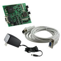
DEMO BOARD FOR PCA9564
Manufacturer
NXP Semiconductors
Datasheet
1.OM6277598.pdf
(52 pages)
Specifications of OM6277,598
Main Purpose
Interface, I2C Controller
Embedded
Yes, MCU, 8-Bit
Utilized Ic / Part
PCA9564
Primary Attributes
I2C Bus Controller, 1 8-Bit GPIO, 1 8-Bit LED Dimmer
Secondary Attributes
8 Momentary Switches, 23 LEDs
Lead Free Status / RoHS Status
Not applicable / Not applicable
Other names
568-4001
935283226598
935283226598


JP6
(I2C
Connect)
JP7
(I2C
Connect)
JP8
(VDD Conn)
JP9
(PSEN\)
JP10
(RSTISP)
JP11
JP12
(SCLLV)
JP13
(SDALV)
JP14
JP15
(VDDISP)
JP16
JP17
(Tx ↔Rx)
JP18
(Rx ↔Tx)
JP19
(A0)
JP20
(A1)
JP21
(A2)
VDDMCU+
PORT1LV51
PORT0LPC
Connect I
I
Connect I
I
Power supply for the
I
89C51Rx+/Rx2/66x
(Not applicable to
P89LV51RD2, only to
5 V devices)
P89LPC932 ISP mode
PCA9554A Interrupt
output monitoring
P89x51 with I
connection to I
P89x51 with I
connection to I
PCA9564 control signals
PCA9564 parallel bus
Connection TxD
P89LV51RD2 to RxD
P89LPC932
Connection RxD
P89LV51RD2 to TxD
P89LPC932
P89LPC932 I
address input 0
P89LPC932 I
address input 1
P89LPC932 I
address input 2
P89xx51 Power supply
selection
Port 1 P89LV51
Port 0 P89LPC932
ISP mode
2
2
2
C-bus 2
C-bus 2
C-bus connectors
2
2
C-bus 1 and
C-bus 1 and
2
2
2
2
2
C slave
C slave
C slave
C-bus
2
C-bus
2
C-bus 2
C-bus 2
Table 2. PCA9564 Evaluation Jumpers and Headers
Open
Closed
Open
Closed
Open
Closed
Open
Closed
Open
Closed
Open
Closed between 1 and 2
(INTLPC)
Closed between 2 and 3
(INTLV)
Open
Closed
Open
Closed
Open
Closed
Open
Closed
Open
Closed
Open
Closed
Open
Closed
Open
Closed
Open
Closed
7
SCL I
SCL I
SDA I
SDA I
Pins connected together
Pins connected together
Address Input 0 connected to GND – A0 = 0
Address Input 1 connected to GND – A1 = 0
Address Input 2 connected to GND – A2 = 0
V
supply
V
ISP mode not entered
ISP mode entered
Note: More information can be found on the Philips Application
Normal mode
P89LPC932 ISP mode
PCA9554A
PCA9554A
PCA9554A
P89C51Rx+/Rx2/66x with I
SCL I
P89C51Rx+/Rx2/66x with I
I
P89C51Rx+/Rx2/66x with I
SDA I
P89C51Rx+/Rx2/66x with I
I
Probing of PCA9564 control signals
P89LPC932 ISP mode
Normal mode
Probing of PCA9564 8-bit parallel bus
Pins not connected together
Note: JP2 and JP3 must be open when JP17 is closed
Pins not connected together
Note: JP2 and JP3 must be open when JP18 is closed
Address Input 0 connected to V
Address Input 1 connected to V
Address Input 2 connected to V
External power supply can be applied to the P89xx51 microcontroller
(Voltage applied to pin VDDMCU+, on the left side of the jumper)
Internal regulated 3.3 V power supply applied to the P89xx51
microcontroller
General purpose 8-bit Input/Output port (Port 1 P89LV51RD2)
General purpose 8-bit Input/Output port (Port 0 P89LPC932)
2
2
C-bus 2
C-bus 2
DD
DD
pin of connectors not connected to the internal 3.3 V power
pin of connectors connected to the internal 3.3 V power supply
2
2
2
2
2
2
Notes AN461: “In-circuit and In-application programming of
the 89C51Rx+/Rx2/66x microcontrollers”
C-bus 1 and SCL I
C-bus 1 and SCL I
C-bus 2
C-bus 1 and SDA I
C-bus 1 and SDAI
C-bus 2
INT
INT
INT
pin not monitored
pin can be monitored by P89LPC932
pin can be monitored by P89LV51RD2
2
2
2
C-bus 2 are not connected together
C-bus 2 are connected together
2
C-bus 2 are connected together
C-bus 2 are not connected together
2
2
2
2
C-bus (SCL = P1.6) not connected to
C-bus (SCL = P1.6) connected to SCL
C-bus (SDA = P1.7) not connected to
C-bus (SDA = P1.7) connected to SDA
DD
DD
DD
– A0 = 1
– A1 = 1
– A2 = 1
Related parts for OM6277,598
Image
Part Number
Description
Manufacturer
Datasheet
Request
R

Part Number:
Description:
Display Modules & Development Tools I2C BUS CONTROLLER EVAL BOARD
Manufacturer:
NXP Semiconductors

Part Number:
Description:
NXP Semiconductors designed the LPC2420/2460 microcontroller around a 16-bit/32-bitARM7TDMI-S CPU core with real-time debug interfaces that include both JTAG andembedded trace
Manufacturer:
NXP Semiconductors
Datasheet:

Part Number:
Description:
NXP Semiconductors designed the LPC2458 microcontroller around a 16-bit/32-bitARM7TDMI-S CPU core with real-time debug interfaces that include both JTAG andembedded trace
Manufacturer:
NXP Semiconductors
Datasheet:
Part Number:
Description:
NXP Semiconductors designed the LPC2468 microcontroller around a 16-bit/32-bitARM7TDMI-S CPU core with real-time debug interfaces that include both JTAG andembedded trace
Manufacturer:
NXP Semiconductors
Datasheet:
Part Number:
Description:
NXP Semiconductors designed the LPC2470 microcontroller, powered by theARM7TDMI-S core, to be a highly integrated microcontroller for a wide range ofapplications that require advanced communications and high quality graphic displays
Manufacturer:
NXP Semiconductors
Datasheet:
Part Number:
Description:
NXP Semiconductors designed the LPC2478 microcontroller, powered by theARM7TDMI-S core, to be a highly integrated microcontroller for a wide range ofapplications that require advanced communications and high quality graphic displays
Manufacturer:
NXP Semiconductors
Datasheet:
Part Number:
Description:
The Philips Semiconductors XA (eXtended Architecture) family of 16-bit single-chip microcontrollers is powerful enough to easily handle the requirements of high performance embedded applications, yet inexpensive enough to compete in the market for hi
Manufacturer:
NXP Semiconductors
Datasheet:
Part Number:
Description:
The XA-S3 device is a member of Philips Semiconductors? XA(eXtended Architecture) family of high performance 16-bitsingle-chip microcontrollers
Manufacturer:
NXP Semiconductors
Datasheet:

Part Number:
Description:
The NXP BlueStreak LH75401/LH75411 family consists of two low-cost 16/32-bit System-on-Chip (SoC) devices
Manufacturer:
NXP Semiconductors
Datasheet:
Part Number:
Description:
The NXP LPC3130/3131 combine an 180 MHz ARM926EJ-S CPU core, high-speed USB2
Manufacturer:
NXP Semiconductors
Datasheet:
Part Number:
Description:
The NXP LPC3141 combine a 270 MHz ARM926EJ-S CPU core, High-speed USB 2
Manufacturer:
NXP Semiconductors
Part Number:
Description:
The NXP LPC3143 combine a 270 MHz ARM926EJ-S CPU core, High-speed USB 2
Manufacturer:
NXP Semiconductors

Part Number:
Description:
The NXP LPC3152 combines an 180 MHz ARM926EJ-S CPU core, High-speed USB 2
Manufacturer:
NXP Semiconductors
Part Number:
Description:
The NXP LPC3154 combines an 180 MHz ARM926EJ-S CPU core, High-speed USB 2
Manufacturer:
NXP Semiconductors