AD5259EVAL Analog Devices Inc, AD5259EVAL Datasheet - Page 14
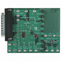
AD5259EVAL
Manufacturer Part Number
AD5259EVAL
Description
BOARD EVAL FOR AD5259 DGTL POT
Manufacturer
Analog Devices Inc
Datasheet
1.AD5259BRMZ10.pdf
(24 pages)
Specifications of AD5259EVAL
Main Purpose
Digital Potentiometer
Utilized Ic / Part
AD5259
Lead Free Status / RoHS Status
Contains lead / RoHS non-compliant
Secondary Attributes
-
Embedded
-
Primary Attributes
-
Lead Free Status / Rohs Status
Not Compliant


AD5259
THEORY OF OPERATION
The AD5259 is a 256-position digitally-controlled variable
resistor (VR) device. EEPROM is pre-loaded at midscale from
the factory, and initial power-up is, accordingly, at midscale.
PROGRAMMING THE VARIABLE RESISTOR
Rheostat Operation
The nominal resistance (R
and Terminal B is available in 5 kΩ, 10 kΩ, 50 kΩ, and 100 kΩ.
The nominal resistance of the VR has 256 contact points accessed
by the wiper terminal. The 8-bit data in the RDAC latch is
decoded to select one of 256 possible settings.
The general equation determining the digitally programmed
output resistance between Wiper W and Terminal B is
where:
D is the decimal equivalent of the binary code loaded in the
8-bit RDAC register.
R
R
each internal switch.
In the zero-scale condition, there is a relatively low value finite
wiper resistance. Care should be taken to limit the current flow
between Wiper W and Terminal B in this state to a maximum
pulse current of no more than 20 mA. Otherwise, degradation
or destruction of the internal switch contact can occur.
AB
W
is the wiper resistance contributed by the ON resistance of
is the end-to-end resistance.
R
WB
(
D
A
B
)
Figure 39. AD5259 Equivalent RDAC Circuit
Figure 38. Rheostat Mode Configuration
256
D7
D6
D5
D4
D3
D2
D1
D0
DECODER
D
W
LATCH
RDAC
AND
R
AB
AB
A
B
) of the RDAC between Terminal A
2
R
R
R
R
S
S
S
S
R
W
W
A
B
A
W
B
W
Rev. B | Page 14 of 24
(1)
Similar to the mechanical potentiometer, the resistance of the
RDAC between Wiper W and Terminal A produces a digitally
controlled complementary resistance, R
setting for R
decreases as the data loaded in the latch increases in value.
The general equation for this operation is
Typical device-to-device matching is process lot dependent and
may vary by up to ±30%. For this reason, resistance tolerance is
stored in the EEPROM, enabling the user to know the actual
R
PROGRAMMING THE POTENTIOMETER DIVIDER
Voltage Output Operation
The digital potentiometer easily generates a voltage divider at
Wiper W to Terminal B and Wiper W to Terminal A propor-
tional to the input voltage at Terminal A to Terminal B. Unlike
the polarity of V
across Terminal A to Terminal B, Wiper W to Terminal A, and
Wiper W to Terminal B can be at either polarity.
If ignoring the effect of the wiper resistance for approximation,
connecting the A terminal to 5 V and the B terminal to ground
produces an output voltage at Wiper W to Terminal B starting
at 0 V up to 1 LSB less than 5 V. The general equation defining
the output voltage at V
input voltage applied to Terminal A and Terminal B is
A more accurate calculation, which includes the effect of wiper
resistance, V
Operation of the digital potentiometer in the divider mode
results in a more accurate operation over temperature. Unlike
the rheostat mode, the output voltage is dependent mainly
on the ratio of the Internal Resistors R
the absolute values.
AB
within 0.1%.
V
V
R
WA
W
W
(
(
D
D
(
D
)
)
)
WA
W
Figure 40. Potentiometer Mode Configuration
, is
256
R
starts at a maximum value of resistance and
D
256
WB
DD
R
256
AB
V
(
to GND, which must be positive, voltage
D
A
)
D
W
V
V
I
256
A
with respect to ground for any valid
R
256
AB
R
WA
A
B
D
R
AB
2
V
(
D
W
B
)
R
V
W
B
WA
V
WA
O
and R
. The resistance value
WB
and not
(2)
(3)
(4)
Related parts for AD5259EVAL
Image
Part Number
Description
Manufacturer
Datasheet
Request
R


Part Number:
Description:
±1.7g Dual-Axis IMEMS Accelerometer Evaluation Board
Manufacturer:
Analog Devices Inc
Datasheet:

Part Number:
Description:
Inertial Sensor Evaluation System
Manufacturer:
Analog Devices Inc
Datasheet:
Part Number:
Description:
Manufacturer:
Analog Devices Inc
Datasheet:
Part Number:
Description:
Manufacturer:
Analog Devices Inc
Datasheet:
Part Number:
Description:
Manufacturer:
Analog Devices Inc
Datasheet:
Part Number:
Description:
Manufacturer:
Analog Devices Inc
Datasheet:
Part Number:
Description:
Manufacturer:
Analog Devices Inc
Datasheet:
Part Number:
Description:
Manufacturer:
Analog Devices Inc
Datasheet:
Part Number:
Description:
Manufacturer:
Analog Devices Inc
Datasheet:
Part Number:
Description:
Manufacturer:
Analog Devices Inc
Datasheet:
Part Number:
Description:
Manufacturer:
Analog Devices Inc
Datasheet:
Part Number:
Description:
Manufacturer:
Analog Devices Inc
Datasheet: