AD5259EVAL Analog Devices Inc, AD5259EVAL Datasheet - Page 2
AD5259EVAL
Manufacturer Part Number
AD5259EVAL
Description
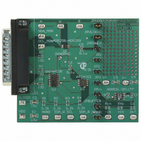
BOARD EVAL FOR AD5259 DGTL POT
Manufacturer
Analog Devices Inc
Datasheet
1.AD5259BRMZ10.pdf
(24 pages)
Specifications of AD5259EVAL
Main Purpose
Digital Potentiometer
Utilized Ic / Part
AD5259
Lead Free Status / RoHS Status
Contains lead / RoHS non-compliant
Secondary Attributes
-
Embedded
-
Primary Attributes
-
Lead Free Status / Rohs Status
Not Compliant


AD5259
TABLE OF CONTENTS
Specifications ..................................................................................... 3
Absolute Maximum Ratings ............................................................ 6
Pin Configuration and Function Descriptions ............................. 7
Typical Performance Characteristics ............................................. 8
Test Circuits ..................................................................................... 13
Theory of Operation ...................................................................... 14
I
REVISION HISTORY
5/10—Rev. A to Rev. B
Changes to Figure 5 .......................................................................... 7
Changes to Storing/Restoring Section ......................................... 15
Changes to Table 7 .......................................................................... 16
Changes to Table 14 ........................................................................ 17
Updated Outline Dimensions ....................................................... 21
7/05—Rev. 0 to Rev. A
Added 10-Lead LFCSP ....................................................... Universal
Changes to Features Section and
General Description Section ........................................................... 1
Changes to Table 1 ............................................................................ 3
Changes to Table 2 and Added Figure 4 ........................................ 5
Changes to Table 4 ............................................................................ 7
Changes to Figure 27 Caption ....................................................... 11
Changes to Theory of Operation Section .................................... 14
Changes to I
Changes to Table 5 .......................................................................... 16
Changes to Multiple Devices on One Bus Section ..................... 19
Updated Figure 49 Caption ........................................................... 21
Changes to Ordering Guide .......................................................... 21
2/05—Revision 0: Initial Version
2
C-Compatible Interface............................................................... 15
Electrical Characteristics ............................................................. 3
Timing Characteristics ................................................................ 5
ESD Caution .................................................................................. 6
Programming the Variable Resistor ......................................... 14
Programming the Potentiometer Divider ............................... 14
Writing ......................................................................................... 15
Storing/Restoring ....................................................................... 15
Reading ........................................................................................ 15
2
C-Compatible Interface Section ............................ 15
Rev. B | Page 2 of 24
I
Display Applications ...................................................................... 20
Outline Dimensions ....................................................................... 21
2
C-Compatible Format ................................................................. 16
Generic Interface ........................................................................ 16
Write Modes ................................................................................ 16
Read Modes ................................................................................. 17
Store/Restore Modes .................................................................. 17
Tolerance Readback Modes ...................................................... 18
ESD Protection of Digital Pins and Resistor Terminals ........ 19
Power-Up Sequence ................................................................... 19
Layout and Power Supply Bypassing ....................................... 19
Multiple Devices on One Bus ................................................... 19
Evaluation Board ........................................................................ 19
Circuitry ...................................................................................... 20
Ordering Guide .......................................................................... 22
Related parts for AD5259EVAL
Image
Part Number
Description
Manufacturer
Datasheet
Request
R


Part Number:
Description:
±1.7g Dual-Axis IMEMS Accelerometer Evaluation Board
Manufacturer:
Analog Devices Inc
Datasheet:

Part Number:
Description:
Inertial Sensor Evaluation System
Manufacturer:
Analog Devices Inc
Datasheet:
Part Number:
Description:
Manufacturer:
Analog Devices Inc
Datasheet:
Part Number:
Description:
Manufacturer:
Analog Devices Inc
Datasheet:
Part Number:
Description:
Manufacturer:
Analog Devices Inc
Datasheet:
Part Number:
Description:
Manufacturer:
Analog Devices Inc
Datasheet:
Part Number:
Description:
Manufacturer:
Analog Devices Inc
Datasheet:
Part Number:
Description:
Manufacturer:
Analog Devices Inc
Datasheet:
Part Number:
Description:
Manufacturer:
Analog Devices Inc
Datasheet:
Part Number:
Description:
Manufacturer:
Analog Devices Inc
Datasheet:
Part Number:
Description:
Manufacturer:
Analog Devices Inc
Datasheet:
Part Number:
Description:
Manufacturer:
Analog Devices Inc
Datasheet: