RDK-128 Power Integrations, RDK-128 Datasheet - Page 8
RDK-128
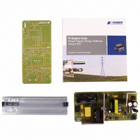
Manufacturer Part Number
RDK-128
Description
KIT REF DESIGN 36-72W MOTOR DRVR
Manufacturer
Power Integrations
Specifications of RDK-128
Main Purpose
Power Management, Motor Control
Embedded
No
Utilized Ic / Part
PKS606
Primary Attributes
Variable Speed 12V 36W DC Motor, 90 ~ 265 VAC
Secondary Attributes
External Potentiometer or Variable DC Voltage Speed Control
Lead Free Status / RoHS Status
Not applicable / Not applicable
Other names
596-1198


RDR-128 36 W, 72 W Peak Variable Output Power Supply
If the EN/UV pin has not been pulled low for 30 ms and the input voltage is below the
under-voltage threshold, then the loss of regulation is assumed to be due to a low line
condition, and the PeakSwitch will stop switching until the under-voltage threshold is
exceeded again.
4.4 Output Rectification and Filtering
Diode D9 rectifies the output voltage while capacitors C13 and C14 provide output
filtering. The output capacitor current ripple rating is chosen to be sufficient for the
maximum rated continuous/average load. Resistor R9 and capacitor C11 form a snubber
network across diode D9, which reduces high frequency ringing that occurs during the
diode turn off event.
4.5 Output Feedback
The PeakSwitch family of devices uses a simple on/off control scheme. When a current
greater than 240 µA is drawn from the EN/UV pin of U1, the subsequent switching cycle
is disabled.
optocoupler conducts enough current through R8, thus forward biasing D8 and turning on
transistor Q1.
phototransistor’s collector connected to the bypass pin of the PeakSwitch gives a
collector to emitter voltage (V
to source current more effectively while using the high gain, small signal transistor Q1 to
draw the current from the EN/UV pin. Optocoupler U2’s high CTR (300% – 600%)
ensures a fast control loop response. Diode D8 is placed close to Q1 and thus provides
thermal compensation against Q1’s V
The output voltage is variable to allow for speed control of the DC motor. An adjustable
shunt regulator, U3, has its cathode tied to its reference, making it behave as a voltage
reference at approximately 1.24 V above the 1.1 V optocoupler’s LED (U2A) drop.
When no external control voltage is applied at terminals J3, diode D10 remains reverse
biased and potentiometer R12 controls the voltage of the divider network formed by itself,
R13 and R10. Decreasing the value of R12 programs a new voltage set-point (and also
a new speed), and the feedback loop now regulates to a lower output voltage. Setting
potentiometer R12 to its minimum value regulates the output down to 2.35 V. An 11 V
zener diode (VR2) is in place to ensure the output voltage does not regulate too far
above 12 V, as may occur due to the large tolerances of most potentiometers (which may
be as high as ±20%).
The supply’s output voltage may also be controlled by an external DC control voltage
applied at J3, with amplitude between 0 V and 10 V. Applying an external voltage above
3.5 V at J3 will forward bias diode D10 and will set the reference and cathode pin of the
shunt regulator to the external control voltage. Applying a higher external control voltage
allows more current to flow through the LED of the optocoupler and thus reduces the
supply’s output voltage. If 10 V is applied at J3, the supply shuts down completely.
Reducing the external control voltage after a shut down will start the power supply again.
Power Integrations, Inc.
Tel: +1 408 414 9200 Fax: +1 408 414 9201
www.powerint.com
The EN/UV pin is pulled low whenever phototransistor U2B of the
Transistor Q1 then pulls current out of the EN/UV pin.
CE
) of approximately 5.8 V, which allows the phototransistor
BE
drop.
Page 8 of 32
Having the
16-Aug-07
Related parts for RDK-128
Image
Part Number
Description
Manufacturer
Datasheet
Request
R

Part Number:
Description:
KIT REF DESIGN FOR LNK457D
Manufacturer:
Power Integrations
Datasheet:

Part Number:
Description:
REFERENCE DESIGN LINKSWITCH-PH
Manufacturer:
Power Integrations
Datasheet:

Part Number:
Description:
KIT REF DESIGN FOR LNK403EG
Manufacturer:
Power Integrations
Datasheet:

Part Number:
Description:
KIT REF DESIGN FOR LNK406EG
Manufacturer:
Power Integrations
Datasheet:

Part Number:
Description:
KIT REF DESIGN LINKSWITCH-CV
Manufacturer:
Power Integrations
Datasheet:

Part Number:
Description:
KIT REF DESIGN LINKSWITCH 2
Manufacturer:
Power Integrations
Datasheet:

Part Number:
Description:
Specifications: Family: Eval Boards - DC/DC & AC/DC (Off-Line) SMPS ; Series: HiperLCS™ ; Main Purpose: DC/DC, Step Down ; Outputs and Type: 1, Isolated ; Power - Output: 150W ; Voltage - Output: 24V ; Current - Output: 6.25A ; Voltage - Input:
Manufacturer:
Power Integrations, Inc.
Datasheet:

Part Number:
Description:
KIT DESIGN REF TINYSWITCH-III
Manufacturer:
Power Integrations
Datasheet:

Part Number:
Description:
KIT DESIGN REF LINKSWITCH LP
Manufacturer:
Power Integrations
Datasheet:

Part Number:
Description:
KIT REF DESIGN LED LINKSWITCH TN
Manufacturer:
Power Integrations
Datasheet:
Part Number:
Description:
KIT REF DESIGN FOR LNK457D
Manufacturer:
Power Integrations
Datasheet:
Part Number:
Description:
REFERENCE DESIGN LINKSWITCH-PH
Manufacturer:
Power Integrations
Datasheet:
Part Number:
Description:
Specifications: Manufacturer: Power Integrations ; Output Voltage: 380 VDC ; Input / Supply Voltage (Max): 264 VAC ; Input / Supply Voltage (Min): 90 VAC ; Mounting Style: Through Hole ; Output Current: 0.913 A ; Output Power: 347 W
Manufacturer:
Power Integrations, Inc.
Part Number:
Description:
Specifications: Family: Eval Boards - DC/DC & AC/DC (Off-Line) SMPS ; Series: HiperLCS™ ; Main Purpose: DC/DC, Step Down ; Outputs and Type: 1, Isolated ; Power - Output: 150W ; Voltage - Output: 24V ; Current - Output: 6.25A ; Voltage - Input:
Manufacturer:
Power Integrations, Inc.
Datasheet: