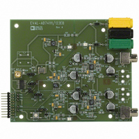
EVAL-AD74111EBZ Analog Devices Inc, EVAL-AD74111EBZ Datasheet - Page 4
EVAL-AD74111EBZ
Manufacturer Part Number
EVAL-AD74111EBZ
Description
BOARD EVAL FOR AD74111
Manufacturer
Analog Devices Inc
Specifications of EVAL-AD74111EBZ
Main Purpose
Interface, Analog Front End (AFE)
Utilized Ic / Part
AD74111
Lead Free Status / RoHS Status
Lead free / RoHS Compliant
Secondary Attributes
-
Embedded
-
Primary Attributes
-
Lead Free Status / Rohs Status
Supplier Unconfirmed


EVAL-AD74111EB
EVALUATION BOARD SOFTWARE
DSP EXAMPLES
The following text gives some code examples showing methods
of interfacing the AD74111 to Analog Devices, Inc. ’ s fixed-point
DSPs. The flowcharts are generic and should be adaptable to
any type of DSP, but the code samples are specifically for the
ADSP-218x DSPs.
INTERRUPTS
The code examples that follow make use of the serial port
(SPORT) transmit and receive interrupts that allow the processor
to service the codec only when required. The transmit section
of the ADSP-218x SPORT consists of a transmit register, Tx0
for SPORT0 and Tx1 for SPORT1, and a serial shift register, Rx0
for SPORT0 and Rx1 for SPORT1. Transmission of a data-word
is initiated by loading it to the appropriate Tx register. The DSP
begins transmitting this word by copying it to the serial shift
register where it is clocked out one bit at a time dependant on
the SCLK rate. A transmit interrupt occurs when it is safe to
load the Tx register with the next value to be transmitted. The
DSP will not allow the second word to be transmitted until the
first word is completely transmitted. A transmit interrupt
occurs when the second bit of the data-word is transmitted.
A receive interrupt occurs when a complete data-word is
received into the Receive Register Rx0 or the Receive Register
Rx1. The receive section of the SPORT has a similar serial shift
register to the transmit section. It is important that any data
received in the Rx register be read as soon as possible because a
new word can be read into the serial shift register and overwrite
the Rx register once the entire word is received.
16-BIT MIXED MODE, 16-BIT DATA, MASTER MODE
The flowchart in Figure 6 is an example of how to interface the
DSP to the AD74111 in master mode. In master mode, the
codec generates the DFS and DCLK signals so the TFS1/RFS1
and SCLK1 are inputs to the DSP. The codec is operating in its
default 16-bit mixed mode with the data-word length set to 16
bits. In this mode, the AD74111 generates two DFS pulses per
sample interval, one for the control register/status information,
and one for the DAC/ADC data.
These software examples take the ADC results and send them
back to the DAC to create a loopback effect. The DAC output is
therefore one sample interval behind the ADC input.
Rev. 0 | Page 4 of 16
The software uses three buffers to control the flow of information:
1. The control buffer contains the control register words that
2. The Tx buffer contains a control register value and a value for
3. The Rx buffer stores the status information and the ADC result.
Figure 5 shows how the buffers are arranged in memory.
When the program is running, the transmit interrupt reads the
next value in the Tx buffer and transmit it when it receives a
transmit interrupt. The receive interrupt does most of the work
in this example. When a receive interrupt is generated, the
program reads the value from the Rx1 register into the AY1
register immediately storing it for later use. It then decrements
and checks a counter value to determine how many receive
interrupts have been received in the current sample interval. If
the value is not zero, the control word just finishes transmitting,
and the status word is just received. The status information is
not required in this example; therefore, the program returns from
the interrupt subroutine and waits for the next interrupt event.
When the program determines that two receive interrupts have
occurred (control counter = 0), it will get the next control word
to be sent to the codec from control buffer and load it to the
CTRL memory location in the Tx buffer. The ADC value that
was just received is copied to the DAC memory location to
create a loopback operation, and this value is transmitted to
the DAC in the next sample interval. The program resets the
control counter variable and returns from the interrupt
subroutine to wait for the next interrupt event.
need to be sent to the AD74111.
the DAC.
CONTROL-
BUFFER
Rx
Tx
Figure 5. Buffer Memory Map
CONTROL COUNTER
REG DATA 1
REG DATA 2
REG DATA 3
REG DATA 4
REG DATA 5
REG DATA 6
REG DATA 7
REG DATA 8
STATUS
CTRL
ADC
DAC
I1
I2
I1
Related parts for EVAL-AD74111EBZ
Image
Part Number
Description
Manufacturer
Datasheet
Request
R


Part Number:
Description:
BOARD EVAL FOR SI270X-A
Manufacturer:
Silicon Laboratories Inc
Datasheet:

Part Number:
Description:
BUCK CONV REF DESIGN KIT IP1201
Manufacturer:
International Rectifier
Datasheet:
Part Number:
Description:
BOARD DEMO SYNC DUAL BUCK CNVTER
Manufacturer:
International Rectifier
Datasheet:
Part Number:
Description:
BOARD DEMO SYNC BUCK CONVETER
Manufacturer:
International Rectifier
Datasheet:

Part Number:
Description:
EVALBOARD/EB Omnidirectional microphone - Analog
Manufacturer:
Analog Devices
Datasheet:
Part Number:
Description:
EVALBOARD/EB Omnidirectional microphone - Analog
Manufacturer:
Analog Devices
Datasheet:


Part Number:
Description:
BOARD EVAL LED DRIVER LT3756
Manufacturer:
Linear Technology
Datasheet:

Part Number:
Description:
BOARD EVAL FOR AD7741/7742
Manufacturer:
Analog Devices Inc
Datasheet:

Part Number:
Description:
±1.7g Dual-Axis IMEMS Accelerometer Evaluation Board
Manufacturer:
Analog Devices Inc
Datasheet:

Part Number:
Description:
IC MULTIPLIER ANALOG 8-SOIC T/R
Manufacturer:
Analog Devices Inc
Datasheet:

Part Number:
Description:
IC ANALOG MULTIPLIER 8-DIP
Manufacturer:
Analog Devices Inc
Datasheet:
Part Number:
Description:
IC ANALOG MULTIPLIER 8-SOIC
Manufacturer:
Analog Devices Inc
Datasheet:
Part Number:
Description:
IC ANALOG MULTIPLIER 8-DIP
Manufacturer:
Analog Devices Inc
Datasheet: