CDB5467U Cirrus Logic Inc, CDB5467U Datasheet - Page 34
CDB5467U
Manufacturer Part Number
CDB5467U
Description
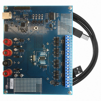
BOARD EVAL FOR CS5467 ADC
Manufacturer
Cirrus Logic Inc
Type
A/Dr
Specifications of CDB5467U
Main Purpose
Power Management, Energy/Power Meter
Embedded
Yes, MCU, 8-Bit
Utilized Ic / Part
CS5467
Primary Attributes
Watt-Hour Meter
Secondary Attributes
Graphical User Interface, SPI™ & USB Interfaces
Product
Data Conversion Development Tools
Maximum Clock Frequency
4 MHz
Interface Type
USB
Supply Voltage (max)
5 V
Supply Voltage (min)
3.3 V
For Use With/related Products
CS5467
Lead Free Status / RoHS Status
Contains lead / RoHS non-compliant
Lead Free Status / RoHS Status
Lead free / RoHS Compliant, Contains lead / RoHS non-compliant
Other names
598-1555
CDB-5467U
CDB-5467U


8.3 Page 1 Registers
8.3.1 DC Offset for Current (I1
8.3.2 Gain for Current (I1
8.3.3 Power Offset (P1
8.3.4 AC Offset for Current (I1
34
MSB
MSB
MSB
MSB
-(2
-(2
-(2
2
1
0
0
0
)
)
)
Address: 0 ( I1
Default = 0
DC offset registers I1
tion, selected registers are written with the inverse of the DC offset measured. The application program can
also write the DC offset register values. These are two's complement values in the range of -1.0 ≤ value < 1.0,
with the binary point to the right of the MSB.
Address: 1 ( I1
Default = 1.0
Gain registers I1
tion, selected register are written with the multiplicative inverse of the gain measured. These are unsigned
fixed-point values in the range of 0 ≤ value < 4.0, with the binary point to the right of the second MSB.
A
Default = 0
Power offset P1
P1
ment values in the range of -1.0 ≤ value < 1.0, with the binary point to the right of the MSB.
Address: 5 ( I1
Default = 0
AC offset registers I1
to the RMS results before being stored to the RMS result registers. They can be used to reduce systematic
errors in the RMS results. These are two's complement values in the range of -1.0 ≤ value < 1.0, with the bi-
nary point to the right of the MSB.
ddress: 4 ( P1
AVG
2
2
2
2
-1
-1
-1
0
( P2
2
2
2
2
AVG
-2
-1
-2
-2
OFF
GAIN
ACOFF
OFF
) register results. It can be used to reduce systematic energy errors. These are two's comple-
OFF
GAIN
2
2
2
2
), 2 ( V1
-3
-2
-3
-3
), 3 ( V1
), 11 ( P2
OFF
( P2
), 6 ( V1
ACOFF
OFF
& V1
GAIN
OFF
, P2
2
2
2
2
-4
& V1
-3
-4
-4
OFF
GAIN
GAIN
, I2
ACOFF
OFF
& V1
) is added to instantaneous power and averaged over a low-rate interval to yield
OFF
ACOFF
OFF
), 7 ( I2
OFF
GAIN
( I2
), 8 ( I2
2
2
2
2
, I2
)
ACOFF
-5
-4
-5
-5
)
GAIN
( I2
, I2
), 12 ( I2
OFF
OFF
) and Voltage (V1
OFF
GAIN
ACOFF
2
2
2
2
& V2
(
-6
-5
-6
-6
V
) and Voltage (V1
), 9 ( V2
ACOFF
& V2
ACOFF
), 10 ( V2
GAIN
) and Voltage (V1
2
2
2
2
OFF
-7
-6
-7
-7
OFF
&
) are initialized to 1.0 on reset. During AC or DC gain calibra-
), 13 ( V2
V2
) are initialized to zero on reset. During DC offset calibra-
GAIN
)
ACOFF
.....
.....
.....
.....
GAIN
)
ACOFF
)
OFF
2
2
2
2
are initialized to zero on reset. These are added
-17
-16
-17
-17
, V2
, V2
)
ACOFF
GAIN
2
2
2
2
-18
-17
-18
-18
OFF
)
, V2
)
2
2
2
2
-19
-18
-19
-19
ACOFF
2
2
2
2
-20
-19
-20
-20
)
2
2
2
2
-21
-20
-21
-21
CS5467
2
2
2
2
-22
-21
-22
-22
DS714F1
LSB
LSB
LSB
LSB
2
2
2
2
-23
-22
-23
-23
Related parts for CDB5467U
Image
Part Number
Description
Manufacturer
Datasheet
Request
R

Part Number:
Description:
Development Kit
Manufacturer:
Cirrus Logic Inc
Datasheet:
Part Number:
Description:
Development Kit
Manufacturer:
Cirrus Logic Inc
Datasheet:


Part Number:
Description:
High-efficiency PFC + Fluorescent Lamp Driver Reference Design
Manufacturer:
Cirrus Logic Inc
Datasheet:
Part Number:
Description:
Development Kit
Manufacturer:
Cirrus Logic Inc
Datasheet:
Part Number:
Description:
Development Kit
Manufacturer:
Cirrus Logic Inc
Datasheet:

Part Number:
Description:
Development Kit
Manufacturer:
Cirrus Logic Inc
Datasheet:
Part Number:
Description:
Development Kit
Manufacturer:
Cirrus Logic Inc
Datasheet:
Part Number:
Description:
Development Kit
Manufacturer:
Cirrus Logic Inc
Datasheet:
Part Number:
Description:
Development Kit
Manufacturer:
Cirrus Logic Inc
Datasheet:

Part Number:
Description:
EVALUATION BOARD FOR CS8427
Manufacturer:
Cirrus Logic Inc
Datasheet:

Part Number:
Description:
BOARD EVAL FOR CS8416 RCVR
Manufacturer:
Cirrus Logic Inc
Datasheet:

Part Number:
Description:
EVALUATION BOARD FOR CS8420
Manufacturer:
Cirrus Logic Inc
Datasheet:

Part Number:
Description:
KIT DEVELOPMENT EP9315 ARM9
Manufacturer:
Cirrus Logic Inc
Datasheet:

Part Number:
Description:
KIT DEVELOPMENT EP9302 ARM9
Manufacturer:
Cirrus Logic Inc
Datasheet: