ADCLK950/PCBZ Analog Devices Inc, ADCLK950/PCBZ Datasheet
ADCLK950/PCBZ
Specifications of ADCLK950/PCBZ


Related parts for ADCLK950/PCBZ


ADCLK950/PCBZ Summary of contents
Page 1
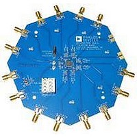
One Technology Way • P.O. Box 9106 • Norwood, MA 02062-9106, U.S.A. • Tel: 781.329.4700 • Fax: 781.461.3113 • www.analog.com Setting Up the Evaluation Board for the ADCLK950 PACKAGE LIST Evaluation board with ADCLK950 component installed Applicable documents (schematic, layout) ...
Page 2
UG-067 TABLE OF CONTENTS Package List ....................................................................................... 1 General Description ......................................................................... 1 Digital Picture of Evaluation Board ............................................... 1 Revision History ............................................................................... 2 Evaluation Board Hardware ............................................................ 3 REVISION HISTORY 11/09—Revision 0: Initial Version Evaluation Board User Guide Recommended Board ...
Page 3
Evaluation Board User Guide EVALUATION BOARD HARDWARE RECOMMENDED BOARD SETUP The recommended setup for the ADCLK950 evaluation board is shown in Figure set to 3.3 V and V CC The CLKSEL jumper (P2) is provided to select ...
Page 4
UG-067 CLOCK OUTPUTS The ADCLK950 has 10 differential outputs. The five even-ordered differential clock outputs on the evaluation board are biased to GND via 200 Ω and ac-coupled to the SMAs. From the SMAs, use matched 50 Ω coaxial cables ...
Page 5
Evaluation Board User Guide EVALUATION BOARD SCHEMATIC AND ARTWORK Z5.531.3425.0 4 VEE 3 2 GND 1 VCC 200 200 R5 R6 200 200 R2 R1 .1UF .1UF C40 C42 .1UF .1UF C39 C41 .1UF .1UF C38 C37 .1UF 10UF .1UF ...
Page 6
UG-067 Evaluation Board User Guide Figure 5. Top Trace Layer Figure 6. Ground Plane Layer Rev Page ...
Page 7
Evaluation Board User Guide Figure 7. V and V Power Plane Layer CC EE Figure 8. Bottom Trace Layer Rev Page UG-067 ...
Page 8
UG-067 NOTES ESD CAUTION Evaluation boards are only intended for device evaluation and not for production purposes. Evaluation boards are supplied “as is” and without warranties of any kind, express, implied, or statutory including, but not limited to, any implied ...