ADCLK950/PCBZ Analog Devices Inc, ADCLK950/PCBZ Datasheet - Page 4
ADCLK950/PCBZ
Manufacturer Part Number
ADCLK950/PCBZ
Description
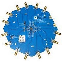
BOARD EVALUATION FOR ADCLK950
Manufacturer
Analog Devices Inc
Series
SIGer
Specifications of ADCLK950/PCBZ
Main Purpose
Timing, Clock Buffer / Driver / Receiver / Translator
Utilized Ic / Part
ADCLK950
Primary Attributes
2 Selectable Inputs, 10 Outputs
Secondary Attributes
LVPECL Output Logic
Silicon Manufacturer
Analog Devices
Application Sub Type
Clock Fanout Buffer
Kit Application Type
Clock & Timing
Silicon Core Number
ADCLK950
Lead Free Status / RoHS Status
Lead free / RoHS Compliant
Embedded
-
Lead Free Status / RoHS Status
Lead free / RoHS Compliant


UG-067
CLOCK OUTPUTS
The
differential clock outputs on the evaluation board are biased to
GND via 200 Ω and ac-coupled to the SMAs. From the SMAs,
use matched 50 Ω coaxial cables into the oscilloscope for
evaluation. The five odd-ordered differential outputs on the
evaluation board are not launched. Use a high bandwidth
differential probe and oscilloscope close to the ADCLK950
device for evaluation. See the evaluation board schematic in
Figure 4 for more details.
ADCLK950
has 10 differential outputs. The five even-ordered
IN_SEL
V
V
CLK0
CLK0
CLK1
CLK1
Figure 3. ADCLK950 1:10 Clock/Data Buffer Block Diagram
REF
REF
V
V
T
T
0
0
1
1
ADCLK950
REFERENCE
REFERENCE
Rev. 0 | Page 4 of 8
Table 2. Power Connections via P1
Label
GND
VCC
VEE
LVPECL
Q0
Q0
Q1
Q1
Q2
Q2
Q3
Q3
Q4
Q4
Q5
Q5
Q6
Q6
Q7
Q7
Q8
Q8
Q9
Q9
Evaluation Board User Guide
ADCLK950
Connect to GND
Connect to 3.3 V
Connect to GND
Related parts for ADCLK950/PCBZ
Image
Part Number
Description
Manufacturer
Datasheet
Request
R

Part Number:
Description:
±1.7g Dual-Axis IMEMS Accelerometer Evaluation Board
Manufacturer:
Analog Devices Inc
Datasheet:

Part Number:
Description:
Inertial Sensor Evaluation System
Manufacturer:
Analog Devices Inc
Datasheet:
Part Number:
Description:
Manufacturer:
Analog Devices Inc
Datasheet:
Part Number:
Description:
Manufacturer:
Analog Devices Inc
Datasheet:
Part Number:
Description:
Manufacturer:
Analog Devices Inc
Datasheet:
Part Number:
Description:
Manufacturer:
Analog Devices Inc
Datasheet:
Part Number:
Description:
Manufacturer:
Analog Devices Inc
Datasheet:
Part Number:
Description:
Manufacturer:
Analog Devices Inc
Datasheet:
Part Number:
Description:
Manufacturer:
Analog Devices Inc
Datasheet:
Part Number:
Description:
Manufacturer:
Analog Devices Inc
Datasheet:
Part Number:
Description:
Manufacturer:
Analog Devices Inc
Datasheet:
Part Number:
Description:
Manufacturer:
Analog Devices Inc
Datasheet:
Part Number:
Description:
Manufacturer:
Analog Devices Inc
Datasheet: