AD8153-EVALZ Analog Devices Inc, AD8153-EVALZ Datasheet - Page 15
AD8153-EVALZ
Manufacturer Part Number
AD8153-EVALZ
Description
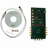
BOARD EVALUATION FOR AD8153
Manufacturer
Analog Devices Inc
Series
XStream™r
Datasheet
1.AD8153ACPZ.pdf
(24 pages)
Specifications of AD8153-EVALZ
Main Purpose
Interface, 2:1 Multiplexer
Embedded
No
Utilized Ic / Part
AD8153
Primary Attributes
Single-Lane 3.2Gbps 2:1 Mux / 1:2 Demux Switch
Secondary Attributes
16 ps Deterministic Jitter, 500 fs rms Random Jitter, GUI via USB
Lead Free Status / RoHS Status
Lead free / RoHS Compliant


I
REGISTER SET
The AD8153 can be controlled in one of three modes: pin
mode, serial mode, and mixed mode. In pin mode, the AD8153
control is derived from the package pins, whereas in serial
mode a set of internal registers controls the AD8153. There is
also a mixed mode where switching is controlled via external
pins, and equalization and pre-emphasis are controlled via the
internal registers. The methods for writing data to and reading
data from the AD8153 are described in the I
section and the I
The mode is controlled via the MODE pin. To set the part in
pin mode, MODE should be driven low to VEE. When MODE
is driven high to VCC, the part is set to serial or mixed mode.
In pin mode, all controls are derived from the external pins. In
serial mode, each channel’s equalization and pre-emphasis are
controlled only through the registers, as described in Table 8.
Additionally, further functionality is available in serial mode as
each channel’s output can be enabled/disabled with the Output
Enable control bits, which is not possible in pin mode. To
change the switching in the AD8153 to serial mode, the mask
bits (Register 0x00) must be set to 1 by writing the value 0x1F to
this register, as explained in the following sections. Once all the
mask bits are set to 1, switching is controlled via the LB_A,
LB_B, LB_C, SEL, and BICAST bits in the register set.
In mixed mode, each channel’s equalization and pre-emphasis
are controlled through the registers as described above. The
switching, however, can be controlled using either the external
Table 8. Register Map
Address
00000000
(0x00)
00000001
(0x01)
00000010
(0x02)
00000011
(0x03)
0000100
(0x04)
2
C SERIAL CONTROL INTERFACE
Bit 7
2
C Data Read section.
Bit 6
Bit 5
Bit 4
BICAST MASK
OUTPUT DISABLE A
OUTPUT DISABLE B
OUTPUT DISABLE C
2
C Data Write
Rev. 0 | Page 15 of 24
Bit 3
SEL MASK
LB_A
LB_B
LB_C
pins or the internal register set. The source of the control is
selected using the mask bits (Register 0x00). If a mask bit is set
to 0, the external pin acts as the source for that specific control.
If a mask bit is set to 1, the associated internal register acts as
the source for that specific control. As an example, if Register 0x00
were set to the value 0x0C, the SEL and LB_C controls would
come from the internal register set (Bit 0 of Register 0x04 and Bit
3 of Register 0x03, respectively), and the BICAST, LB_A, and
LB_B controls would come from the external pins.
GENERAL FUNCTIONALITY
The AD8153 register set is controlled through a 2-wire I
interface. The AD8153 acts only as an I
the I
configure the AD8153 and other I
bus. When the MODE pin is set to a Logic 1, data transfers are
controlled through the use of the two I
pin, SCL, and the bidirectional data pin, SDA.
The AD8153 I
and fast (400 kHz) modes. The SDA line only changes value
when the SCL pin is low with two exceptions. To indicate the
beginning or continuation of a transfer, the SDA pin is driven
low while the SCL pin is high, and to indicate the end of a
transfer, the SDA line is driven high while the SCL line is high.
Therefore, it is important to control the SCL clock to only
toggle when the SDA line is stable unless indicating a start,
repeated start, or stop condition.
Bit 2
LB_C MASK
EQ_B
EQ_C
EQ_A
2
C bus in the system needs to include an I
2
C interface can be run in the standard (100 kHz)
Bit 1
LB_B MASK
PE_A [1]
PE_B [1]
PE_C [1]
BICAST
Bit 0
LB_A MASK
PE_A [0]
PE_B [0]
PE_C [0]
SEL
2
C devices that may be on the
2
2
C slave device. Therefore,
C wires: the input clock
2
C master to
Default
00000000
(0x00)
00000000
(0x00)
00000000
(0x00)
00000000
(0x00)
00000000
(0x00)
AD8153
2
C
Related parts for AD8153-EVALZ
Image
Part Number
Description
Manufacturer
Datasheet
Request
R

Part Number:
Description:
High Output Current Differential Driver
Manufacturer:
Analog Devices
Datasheet:
Part Number:
Description:
High Output Current Differential Driver
Manufacturer:
Analog Devices
Datasheet:

Part Number:
Description:
±1.7g Dual-Axis IMEMS Accelerometer Evaluation Board
Manufacturer:
Analog Devices Inc
Datasheet:

Part Number:
Description:
Inertial Sensor Evaluation System
Manufacturer:
Analog Devices Inc
Datasheet:
Part Number:
Description:
Manufacturer:
Analog Devices Inc
Datasheet:
Part Number:
Description:
Manufacturer:
Analog Devices Inc
Datasheet:
Part Number:
Description:
Manufacturer:
Analog Devices Inc
Datasheet:
Part Number:
Description:
Manufacturer:
Analog Devices Inc
Datasheet:
Part Number:
Description:
Manufacturer:
Analog Devices Inc
Datasheet:
Part Number:
Description:
Manufacturer:
Analog Devices Inc
Datasheet:
Part Number:
Description:
Manufacturer:
Analog Devices Inc
Datasheet:
Part Number:
Description:
Manufacturer:
Analog Devices Inc
Datasheet:
Part Number:
Description:
Manufacturer:
Analog Devices Inc
Datasheet: