CDB42L51 Cirrus Logic Inc, CDB42L51 Datasheet
CDB42L51
Specifications of CDB42L51


Related parts for CDB42L51


CDB42L51 Summary of contents
Page 1
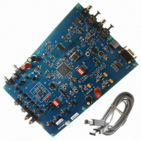
... MCLK Oscillator (socket) http://www.cirrus.com Description The CDB42L51 evaluation board is an excellent means for evaluating the CS42L51 CODEC. Evaluation re- quires an analog/digital signal source and analyzer, and power supplies. Optionally, a Windows PC-compatible computer may be used to evaluate the CS42L51 in Soft- ware Mode. ...
Page 2
... DAC Volume Controls Tab ........................................................................................................... 11 2.5 Register Maps Tab ....................................................................................................................... 12 3. HARDWARE MODE CONTROL ......................................................................................................... 13 3.1 FPGA H/W Control ....................................................................................................................... 13 3.2 CS42L51 H/W Control .................................................................................................................. 17 4. SYSTEM CONNECTIONS AND JUMPERS ....................................................................................... 17 5. CDB42L51 BLOCK DIAGRAM ........................................................................................................... 19 6. CDB42L51 SCHEMATICS .................................................................................................................. 20 7. CDB42L51 LAYOUT ........................................................................................................................... 26 8. ERRATA .............................................................................................................................................. 29 9. REVISION HISTORY ........................................................................................................................... 29 LIST OF FIGURES Figure 1 ...
Page 3
... Figure 23. Power (Schematic Sheet 6) ..................................................................................................... 25 Figure 24. Silk Screen............................................................................................................................... 26 Figure 25. Top-Side Layer ........................................................................................................................ 27 Figure 26. Bottom-Side Layer ................................................................................................................... 28 LIST OF TABLES Table 1. MCLK and Clock/Data Routing Options....................................................................................... 13 Table 2. CS42L51 H/W Mode Control........................................................................................................ 17 Table 3. System Connections .................................................................................................................... 17 Table 4. Jumper Settings ........................................................................................................................... 18 DS679DB2 CDB42L51 3 ...
Page 4
... SYSTEM OVERVIEW The CDB42L51 evaluation board is an excellent means for evaluating the CS42L51 CODEC. Digital audio signal interfaces are provided, and an FPGA is used for easily configuring the board. on page 7 and Section 3. “Hardware Mode Control” on page 13 The CDB42L51 schematic set has been partitioned into six pages and is shown in Figures Connections and Jumpers” ...
Page 5
... Section 3. “Hardware Mode Control” on page 13 (Figure 19 on page Section 3. “Hardware Mode Control” on page 13 Section 2. “Software Mode Control” on page 7 provide configuration details. provide configuration details. CDB42L51 21) and a discussion of the digital au- Section 2. “Software provide configuration details. 21) and a discussion of the digital audio Section 2. “ ...
Page 6
... USB and RS-232 Control Port Connectors A graphical user interface is available for the CDB42L51, allowing easy manipulation of each register. This GUI interfaces with the CDB via the USB and RS-232 connectors and controls all Software Mode options. Section 2. “Software Mode Control” on page 7 Simply connect a cable from the USB or RS-232 connector to the PC and launch the Cirrus Logic FlexGUI software to enable software control of the CDB42L51 ...
Page 7
... Set up the CS42L51 in the “CODEC Configurations”, “ADC Volume Controls” or “DAC Volume Controls” tab as desired. 10. Begin evaluating the CS42L51. For quick setup, the CDB42L51 may, alternatively, be configured by loading a predefined sample script file: 11. On the File menu, click "Restore Board Registers..." 12. Browse to Boards\CDB42L51\Scripts\. ...
Page 8
... General Configuration Tab The “General Configuration” tab provides high-level control of signal routing on the CDB42L51. This tab also includes basic controls for the CS42L51 for quickly setting up the CDB42L51 in simple configurations. Sta- tus text detailing the CODEC’s specific configuration is shown in parenthesis or appears directly below the associated control ...
Page 9
... Volume Controls” tab are not accessible unless the SPE (Signal Processing Engine) signal is se- lected. Update - Reads all registers in the CS42L51 and reflects the current values in the GUI. Reset - Resets the CS42L51. DS679DB2 Figure 2. CODEC Configuration Tab CDB42L51 9 ...
Page 10
... Analog Volume Control - Includes all analog volume controls and adjustments for the ADC. Noise Gate Configuration - Includes all configuration settings for the noise gate. Update - Reads all registers in the CS42L51 and reflects the current values in the GUI. Reset - Resets the CS42L51. 10 Figure 3. ADC Volume Controls Tab CDB42L51 DS679DB2 ...
Page 11
... Tone Control - Includes all bass and treble boosting controls and adjustments. BEEP Generator - Includes all configuration settings for the BEEP generator. Update - Reads all registers in the CS42L51 and reflects the current values in the GUI. Reset - Resets the CS42L51. DS679DB2 Figure 4. DAC Volume Controls Tab CDB42L51 11 ...
Page 12
... Register values can be modified bit-wise or byte-wise. For bit-wise, click the appropriate push-button for the desired bit. For byte-wise, the desired hex value can be typed directly into the register address box in the register map. The “FPGA” and “GPIO” tabs may be ignored. 12 Figure 5. Register Maps Tab - CS42L51 CDB42L51 DS679DB2 ...
Page 13
... Control” and “CS42L51 H/W Control.” These switches are enabled in hardware mode only and ignored in software mode. The CDB42L51 automatically enters hardware mode upon initial power up, or when exiting software mode, by terminating the Cirrus FlexGUI software or by disconnecting the RS-232 serial cable. ...
Page 14
... I/O Header MCLK LRCK/SCLK SDOUT SDIN CS8415 RMCK (256Fs) OLRCK/ OSCLK SDOUT (LJ) CS8406 OMCK (256Fs) ILRCK/ ISCLK SDIN (LJ) I/O Header MCLK LRCK/SCLK SDOUT SDIN CDB42L51 Oscillator CS42L51 MCLK LRCK/SCLK SDIN SDOUT Figure 7. Routing 1 Oscillator CS42L51 MCLK LRCK/SCLK SDIN SDOUT Figure 8. Routing 3 DS679DB2 ...
Page 15
... CS8415 CS42L51 RMCK MCLK (256Fs) OLRCK/ LRCK/SCLK OSCLK SDOUT SDIN SDOUT (LJ) CS8406 OMCK (256Fs) ILRCK/ ISCLK SDIN (LJ) I/O Header MCLK LRCK/SCLK SDOUT SDIN CDB42L51 Oscillator CS42L51 MCLK LRCK/SCLK SDIN SDOUT Figure 10. Routing 5 Oscillator CS42L51 MCLK LRCK/SCLK SDIN SDOUT Figure 12. Routing 7 15 ...
Page 16
... CS8415 CS42L51 RMCK MCLK (256Fs) OLRCK/ LRCK/SCLK OSCLK SDOUT SDIN SDOUT (LJ) CS8406 OMCK (256Fs) ILRCK/ ISCLK SDIN (LJ) I/O Header MCLK LRCK/SCLK SDOUT SDIN CDB42L51 Oscillator CS42L51 MCLK LRCK/SCLK SDIN SDOUT Figure 14. Routing 9 Oscillator CS42L51 MCLK LRCK/SCLK SDIN SDOUT Figure 16. Routing 11 DS679DB2 ...
Page 17
... RCA phono jacks for analog input signal to CS42L51. Input Microphone jacks for analog input signal to CS42L51. Output RCA phono jacks for analog outputs. Output Binding Post connected to LM4889 speaker driver for analog outputs. Output Headphone jack for analog outputs. Table 3. System Connections CDB42L51 SIGNAL PRESENT 17 ...
Page 18
... AOUTB (LPF) Connects lowpass filtered AOUTA to RIGHT RCA jack Ω resistor shunted from AOUTA to GND. SHUNTED *Not connected Jumper placed on pin 1. 16 Ω resistor shunted from AOUTB to GND. SHUNTED *Not connected Jumper placed on pin 1. Table 4. Jumper Settings CDB42L51 *Default factory settings DS679DB2 ...
Page 19
... CDB42L51 BLOCK DIAGRAM Software Mode Control Port Reset Hardware Mode Switches S/PDIF Output (CS8406) FPGA S/PDIF Input (CS8415) Reset MCLK Oscillator (socket) I²C/SPI Header Reset MCLK CS42L51 Reset Clocks/Data Header Figure 17. Block Diagram Analog Input (Line + MIC) Analog Output (Line + Headphone) ...
Page 20
... CDB42L51 SCHEMATICS Figure 18. CS42L51 and Analog I/O (Schematic Sheet 1) ...
Page 21
Figure 19. S/PDIF I/O (Schematic Sheet 2) ...
Page 22
Figure 20. FPGA (Schematic Sheet 3) ...
Page 23
Figure 21. Level Shifters & I/O Stake Header (Schematic Sheet 4) ...
Page 24
Figure 22. Control Port I/O (Schematic Sheet 5) ...
Page 25
Figure 23. Power (Schematic Sheet 6) ...
Page 26
... CDB42L51 LAYOUT Figure 24. Silk Screen ...
Page 27
Figure 25. Top-Side Layer ...
Page 28
Figure 26. Bottom-Side Layer ...
Page 29
... Although the CS42L51 does support VL power supply levels of both +1.8 V and +2.5 V, these levels are not sup- ported by the CDB42L51. Accordingly, header J31 (VL) must be set to +3 ensure correct board operation. It should be noted that this restriction is due only to the hardware design of the CDB42L51. The CS42L51’s allowed voltage levels are specified in the CS42L51 data sheet ...