LMX25120967EVAL/NOPB National Semiconductor, LMX25120967EVAL/NOPB Datasheet - Page 5
LMX25120967EVAL/NOPB
Manufacturer Part Number
LMX25120967EVAL/NOPB
Description
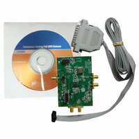
EVALUATION BOARD FOR LMX25120967
Manufacturer
National Semiconductor
Series
PLLatinum™r
Datasheets
1.LMX2512LQ0967NOPB.pdf
(18 pages)
2.LMX2430EVAL.pdf
(8 pages)
3.LMX25120967EVALNOPB.pdf
(24 pages)
Specifications of LMX25120967EVAL/NOPB
Main Purpose
Timing, Frequency Synthesizer
Embedded
No
Utilized Ic / Part
LMX2512
Primary Attributes
Single Fractional-N and Integer-N PLL with VCO
Secondary Attributes
967MHz, CodeLoader Graphical User Interface
Lead Free Status / RoHS Status
Lead free / RoHS Compliant
Other names
*LMX25120967EVAL
*LMX25120967EVAL/NOPB
LMX25120967EVAL
*LMX25120967EVAL/NOPB
LMX25120967EVAL


3.2
The loop bandwidth is the bandwidth of the closed loop PLL system. It is by definition, the
frequency that makes the forward loop gain equal to zero. The spectrum analyzer span is set to
view the characteristic rising, peaking, and falling of the phase noise. Measurement of the loop
bandwidth is rather complex. It is simpler to measure the 0 dB bandwidth. Although, not the
same, the 0 dB bandwidth is a sufficient estimate of the loop filter bandwidth.
bandwidth is defined as the frequency where the phase noise falls back to the level of the close-in
value after rising to its peak value. The value measured is typically greater than the true loop
filter bandwidth. For this evaluation, the 0 dB bandwidth is measured.
3.3
The reference spurs can be seen on a spectrum analyzer and are measured in dBc. The
spectrum analyzer is set to the desired center frequency with a span which allows the reference
sidebands to be viewed. The spurious level is the difference between the level of the VCO output
frequency tone and the level of the spur at an offset equal to the carrier frequency +/- the
comparison frequency.
For a more accurate account of a device’s spurious performance, the reference spurs across the
VCO’s frequency band should be determined. The worst-case spur is typically defined as the
PLL’s spur performance.
3.4
The modulation domain analyzer measures the switching speed, or lock time, using a frequency
versus time plot.
Set the center frequency of the modulation domain analyzer to the final (settling) frequency. Use
a wide span allows viewing of the entire positive or negative switching waveform. Use a narrower
span to evaluate the settling waveform within +/- 1 kHz. A trigger condition, typically a latch
enable pulse, specifies the event that will cause the modulation domain analyzer to capture and
display the measurement results. The lock time is the time difference between the point the
frequency starts to change (T
final value (T
Use the BurstMode tab of the CodeLoader software to program the device to toggle between a
desired minimum and maximum frequency. It is necessary to include a sufficient delay, such as
100000, after each programming command. For more detail, refer to the BurstMode Tab section
in
Communications website: wireless.national.com.
LMX2512LQ0967
the
Loop Filter Bandwidth Measurement
Reference Spur Measurement Using a Spectrum Analyzer
Lock Time Measurement Using a Modulation Domain Analyzer
CodeLoader
2
), (i.e. lock time = T
Operating
LMX2512LQ0967 EVALUATION BOARD OPERATING INSTRUCTIONS
1
), and the point the VCO frequency settles to within +/- 1 kHz of the
2
– T
Instructions
1
).
February 21, 2003
from
National
Semiconductor’s
The 0 dB
Wireless
3
Related parts for LMX25120967EVAL/NOPB
Image
Part Number
Description
Manufacturer
Datasheet
Request
R

Part Number:
Description:
National Semiconductor [8-Bit D/A Converter]
Manufacturer:
National Semiconductor
Datasheet:
Part Number:
Description:
National Semiconductor [Media Coprocessor]
Manufacturer:
National Semiconductor
Datasheet:
Part Number:
Description:
Digitally Controlled Tone and Volume Circuit with Stereo Audio Power Amplifier, Microphone Preamp Stage and National 3D Sound
Manufacturer:
National Semiconductor
Datasheet:
Part Number:
Description:
Digitally Controlled Tone and Volume Circuit with Stereo Audio Power Amplifier, Microphone Preamp Stage and National 3D Sound
Manufacturer:
National Semiconductor
Datasheet:
Part Number:
Description:
AC97 Rev 2 Codec with Sample Rate Conversion and National 3D Sound
Manufacturer:
National Semiconductor
Part Number:
Description:
Manufacturer:
National Semiconductor
Datasheet:
Part Number:
Description:
Manufacturer:
National Semiconductor
Datasheet:
Part Number:
Description:
General Purpose, Low Voltage, Low Power, Rail-to-Rail Output Operational Amplifiers
Manufacturer:
National Semiconductor
Datasheet:
Part Number:
Description:
8-bit 20 MSPS flash A/D converter.
Manufacturer:
National Semiconductor
Datasheet:
Part Number:
Description:
Low Noise Quad Operational Amplifier
Manufacturer:
National Semiconductor
Datasheet:
Part Number:
Description:
Quad Differential Line Receivers
Manufacturer:
National Semiconductor
Datasheet:
Part Number:
Description:
Quad High Speed Trapezoidal? Bus Transceiver
Manufacturer:
National Semiconductor
Datasheet:
Part Number:
Description:
Dual Line Receiver
Manufacturer:
National Semiconductor
Datasheet:
Part Number:
Description:
TTL to 10k ECL Level Translator with Latch
Manufacturer:
National Semiconductor
Datasheet: