LMX25121065EVAL/NOPB National Semiconductor, LMX25121065EVAL/NOPB Datasheet - Page 10
LMX25121065EVAL/NOPB
Manufacturer Part Number
LMX25121065EVAL/NOPB
Description
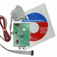
EVALUATION BOARD FOR LMX25121065
Manufacturer
National Semiconductor
Series
PLLatinum™r
Datasheets
1.LMX2512LQ0967NOPB.pdf
(18 pages)
2.LMX2430EVAL.pdf
(8 pages)
3.LMX25121065EVALNOPB.pdf
(24 pages)
Specifications of LMX25121065EVAL/NOPB
Main Purpose
Timing, Frequency Synthesizer
Embedded
No
Utilized Ic / Part
LMX2512
Primary Attributes
Single Fractional-N and Integer-N PLL with VCO
Secondary Attributes
1.065GHz, CodeLoader Graphical User Interface
Lead Free Status / RoHS Status
Lead free / RoHS Compliant
Other names
*LMX25121065EVAL
*LMX25121065EVAL/NOPB
LMX25121065EVAL
*LMX25121065EVAL/NOPB
LMX25121065EVAL


www.national.com
Programming Description
GENERAL PROGRAMMING INFORMATION
The serial interface has a 24-bit shift register to store the incoming data bits temporarily. The incoming data is loaded into the shift
register from MSB to LSB. The data is shifted at the rising edge of the clock signal. When the latch enable signal transitions from
LOW to HIGH, the data stored in the shift register is transferred to the proper register depending on the address bit settings. The
selection of the particular register is determined by the address bits equal to the binary representation of the number of the control
register.
At initial start-up, the MICROWIRE loading requires 4 default words (registers R3, loaded first, to R0, loaded last). After the device
has been initially programmed, the RF VCO frequency can be changed using a single register (R0). If an IF frequency other than
the default value for the device is desired the SPI_DEF bit should be set to 0, the desired values for IF_A, IF_B, and IF_R entered
and words R6 to R0 should be sent.
The control register content map describes how the bits within each control register are allocated to the specific control functions.
NOTE: Bold numbers represent the address bits.
R0
(Default)
R1
(Default)
R2
(Default)
R3
(Default)
R4
R5
R6
MSB
23
SPI_
DEF
IF_
FREQ
[1:0]
IF_
CUR[1:0]
BW_
DUR
[1:0]
0
0
1
22
RF_
SEL
0
0
0
21
RF_
LD
OSC_
FREQ
0
BW_
CRL
[1:0]
0
1
0
20 19
0
1
0
1
1
0
RF_B
[3:0]
0
1
BW_
EN
0
0
0
18 17 16 15 14 13 12
0
0
1
0
0
0
COMPLETE REGISTER MAP
0
0
0
0
0
0
SHIFT REGISTER BIT LOCATION
0
1
1
0
0
RF_A
[2:0]
0
1
1
1
0
IF_A
[3:0]
10
0
1
1
0
0
0
0
1
0
SPUR_
RDT
[1:0]
1
0
0
11
1
1
0
IF_R
10 9 8 7 6 5 4 3
0
0
0
[8:0]
0
IF_B
[8:0]
0 1 0 1 OB_
1 0 1 0 0 0 1
0 0 1 1 0 VCO_
0 0 0 0 0 1 1
RF_FN
[10:0]
CRL
[1:0]
CUR
[1:0]
0 1
RF_
EN
0
2
IF_
EN
0
0
1
1
1
1 0
0 0
0 1
1 0
1 1
1 1
1 1
1 1
LSB
Related parts for LMX25121065EVAL/NOPB
Image
Part Number
Description
Manufacturer
Datasheet
Request
R

Part Number:
Description:
National Semiconductor [8-Bit D/A Converter]
Manufacturer:
National Semiconductor
Datasheet:
Part Number:
Description:
National Semiconductor [Media Coprocessor]
Manufacturer:
National Semiconductor
Datasheet:
Part Number:
Description:
Digitally Controlled Tone and Volume Circuit with Stereo Audio Power Amplifier, Microphone Preamp Stage and National 3D Sound
Manufacturer:
National Semiconductor
Datasheet:
Part Number:
Description:
Digitally Controlled Tone and Volume Circuit with Stereo Audio Power Amplifier, Microphone Preamp Stage and National 3D Sound
Manufacturer:
National Semiconductor
Datasheet:
Part Number:
Description:
AC97 Rev 2 Codec with Sample Rate Conversion and National 3D Sound
Manufacturer:
National Semiconductor
Part Number:
Description:
Manufacturer:
National Semiconductor
Datasheet:
Part Number:
Description:
Manufacturer:
National Semiconductor
Datasheet:
Part Number:
Description:
General Purpose, Low Voltage, Low Power, Rail-to-Rail Output Operational Amplifiers
Manufacturer:
National Semiconductor
Datasheet:
Part Number:
Description:
8-bit 20 MSPS flash A/D converter.
Manufacturer:
National Semiconductor
Datasheet:
Part Number:
Description:
Low Noise Quad Operational Amplifier
Manufacturer:
National Semiconductor
Datasheet:
Part Number:
Description:
Quad Differential Line Receivers
Manufacturer:
National Semiconductor
Datasheet:
Part Number:
Description:
Quad High Speed Trapezoidal? Bus Transceiver
Manufacturer:
National Semiconductor
Datasheet:
Part Number:
Description:
Dual Line Receiver
Manufacturer:
National Semiconductor
Datasheet:
Part Number:
Description:
TTL to 10k ECL Level Translator with Latch
Manufacturer:
National Semiconductor
Datasheet: