M3A-0033 Renesas Electronics America, M3A-0033 Datasheet - Page 18
M3A-0033
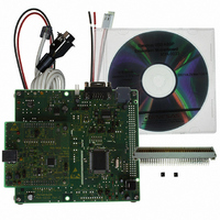
Manufacturer Part Number
M3A-0033
Description
DEV EVALUATION BOARD FOR M66291G
Manufacturer
Renesas Electronics America
Datasheet
1.M3A-0033.pdf
(39 pages)
Specifications of M3A-0033
Main Purpose
USB Controller
Embedded
*
Utilized Ic / Part
M66291
Primary Attributes
*
Secondary Attributes
*
Lead Free Status / RoHS Status
Contains lead / RoHS non-compliant


Chapter 6. Modification of the Setting of the M3A-0033
JP
JP18
JP9
6.1 Changing Power Supply Setting
6.2 Setting for DMA Transfer Using *DREQ
M66291GP Evaluation Board
< Notes in case M3A-0029B is connected >
The power supply to M3A-0033 and M3A-0032, “External power supply (CN1)” or “ Vbus power supply on USB
line” are selectable. Please set up the jumper as Table 6-1.
Table 6-1 Jumper Setting for Supplying Origin of External Power Supply
Note: Please be sure to observe the correct polarity, since this board has no reserve polarity protection.
And, the supply voltage to V
Please set up the jumper as shown in Table 6-2.
Table 6-2 Jumper Setting for Supplying Voltage to IOVCC of M16C/80, M66291GP
- 3.3V is supplied to CoreV
- User should set JP1 of M3A-0032 to “EXIOVCC” side.
Note: Vbus power is then supplied when Vbus is selected as the origin of external power supply.
Table 6-3 shows the supply voltage by the combination of JP5 and JP6 setup.
Table 6-3 Supply voltage by combination of JP5 and JP6
In case M3A-0029B is connected, please be sure to set JP5 to “EX5V” side, JP6 to “3.3V” side.
If it sets up other than the above, M3A-0029B does not operate. Moreover, the worst case, M66290AGP may be
destroyed.
Setting as shown in Table 6-6, *DREQ0 pin and *DREQ1 pin of M66291GP are assigned to *INT1 pin and *INT2
pin of M16C/80 respectively, and DMA transfer can be performed by handshake.
Table 6-4 Jumper Setting of *DREQ0 DMA Transfer
<Notes in case M3A-0029B is connected>
- Since the M66290 needs *Dack for DMA transfer, please short-circuit JP17 (When JP17 is short-circuited, *Dack
pin of M66290A and *CS2 pin of M16C/80 will be connected and JP9 will be invalid).
Supply origin of external power supply
Regulated DC power supply (CN1)
Vbus power supply on USB line
Supply
M66291GP and V
Supply 5. 0V
Supply 3.3V
JP setup
JP5
EX5V
Vbus
Setting
Short-circuit
Set “Dreq1” side
JP6
5.0V
3.3V
5.0V
3.3V
voltage
External power
supply origin
External power
Vbus
supply
CC
to
of M16C/80
CC
IOVCC
CC
of M66291GP for any above-mentioned setup.
of M16C/80 and IOVCC of M66291GP, "5.0V" or "3.3V" is selectable.
Explanation
*DREQ0 pin of M66291GP is connected to *INT1 pin of
M16C/80.
*DREQ1 pin of M66291GP is connected to *INT2 pin of
M16C/80.
of
Supply voltage
M16C/80(M3A-0033)
VCC
5.0V
3.3V
Vbus
3.3V
- 14 -
JP setting
Set JP6 to “5.0V” side (Note).
Set JP6 to “3.3V” side.
JP setting
Set JP5 to "EX5V" side (Note).
Set JP5 to "Vbus" side.
M66291GP (M3A-0032)
IOVCC
5.0V
3.3V
Vbus
3.3V
CoreVCC
3.3V
3.3V
3.3V
3.3V
M3A-0033
Related parts for M3A-0033
Image
Part Number
Description
Manufacturer
Datasheet
Request
R

Part Number:
Description:
DEV EVALUATION BOARD FOR M66592
Manufacturer:
Renesas Electronics America
Part Number:
Description:
DEV EVALUATION KIT FOR M66596
Manufacturer:
Renesas Electronics America
Datasheet:
Part Number:
Description:
DEV EVALUATION BOARD FOR M66591G
Manufacturer:
Renesas Electronics America
Part Number:
Description:
M35054/M35055-XXXSP/FP EVAL BOAR
Manufacturer:
Renesas Electronics America
Part Number:
Description:
DEV M35070/71-XXXFP,M35047-XXXFP
Manufacturer:
Renesas Electronics America
Part Number:
Description:
DEV EVALUATION BOARD 38K0/38K2 G
Manufacturer:
Renesas Electronics America

Part Number:
Description:
KIT STARTER FOR M16C/29
Manufacturer:
Renesas Electronics America
Datasheet:

Part Number:
Description:
KIT STARTER FOR R8C/2D
Manufacturer:
Renesas Electronics America
Datasheet:

Part Number:
Description:
R0K33062P STARTER KIT
Manufacturer:
Renesas Electronics America
Datasheet:

Part Number:
Description:
KIT STARTER FOR R8C/23 E8A
Manufacturer:
Renesas Electronics America
Datasheet:

Part Number:
Description:
KIT STARTER FOR R8C/25
Manufacturer:
Renesas Electronics America
Datasheet:
Part Number:
Description:
KIT STARTER H8S2456 SHARPE DSPLY
Manufacturer:
Renesas Electronics America
Datasheet:

Part Number:
Description:
KIT STARTER FOR R8C38C
Manufacturer:
Renesas Electronics America
Datasheet:

Part Number:
Description:
KIT STARTER FOR R8C35C
Manufacturer:
Renesas Electronics America
Datasheet:

Part Number:
Description:
KIT STARTER FOR R8CL3AC+LCD APPS
Manufacturer:
Renesas Electronics America
Datasheet: