CDB5368 Cirrus Logic Inc, CDB5368 Datasheet - Page 11
CDB5368
Manufacturer Part Number
CDB5368
Description
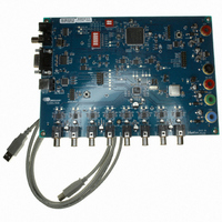
BOARD EVAL FOR CS5368 192KHZ ADC
Manufacturer
Cirrus Logic Inc
Specifications of CDB5368
Number Of Adc's
1
Number Of Bits
24
Sampling Rate (per Second)
192k
Data Interface
Serial
Inputs Per Adc
8 Differential
Input Range
±0.3 V
Voltage Supply Source
Analog and Digital
Operating Temperature
-40°C ~ 85°C
Utilized Ic / Part
CS5368
Description/function
Audio A/D
Operating Supply Voltage
3.3 V
Product
Audio Modules
For Use With/related Products
CS5368
Lead Free Status / RoHS Status
Contains lead / RoHS non-compliant
Lead Free Status / RoHS Status
Lead free / RoHS Compliant, Contains lead / RoHS non-compliant
Other names
598-1157


DS624DB1
4.5
4.6
4.7
4.8
4.9
4.10 Analog Input Buffer
Power Supply Circuitry
Power is applied to the evaluation board through five binding posts (+5 V, +12 V, -12 V, VA and GND). The
GND connection is the common reference for power supplies. The +5 V binding post supplies digital power
for all logic devices. The +12 V and -12 V binding posts supply power for the Operational Amplifier input
buffers. The VA binding posts supplies power to the Analog Reference.
Grounding and Power Supply Treatment
As a high-peformance mixed-signal device, the CS5368 requires careful attention to power and grounding
arrangements to optimize CS5368 performance. The CDB5368 Evaluation Board provides an excellent ref-
erence example of an optimum two-layer board layout that places decoupling capacitors as close to the
CS5368 as possible and provides ground plane fill on both top and bottom layers.
FPGA Hardware
The on-board FPGA is utilized for several purposes. In addition to providing a method for configuring the
CS5368 in Software mode, it contains its own configuration registers that provide clock and data routing for
Master and Slave modes of the CS5368. The FPGA contains a multiplexer that selects which SDOUT line
is routed to the CS8406. It also contains a TDM2PCM engine that extracts channel pairs from a TDM stream
and sends them to the CS8406.
CS8406 S/PDIF Audio Transmitter
The system generates standard S/PDIF data using a CS8406 192 kHz Digital Audio Transmitter. The
CS8406 receives input data from the FPGA in PCM format and transmits S/PDIF data on both optical and
coaxial output connectors. The optical output connector is limited to a maximum speed of 96 kHz. The co-
axial connector supports Quad Speed 192 kHz clocking rates.
Serial Audio Interface
In addition to the standard S/PDIF outputs, the Customer Evaluation Board has been designed to allow
Master and Slave operation using the Serial Audio Interface (SAI) via the 14-pin header, J4, which includes
the signals MCLK, SCLK, LRCK, and the four serial data lines.
When the CS5368 is in Slave mode, SCLK and LRCK/FS must be supplied externally through the J4 head-
er.
The CDB5368 includes an example of an active low-noise, single-ended-to-differential analog input buffer
shown in the schematic drawings,
tial topologies may be used as cost dictates. However, the high performance of the CS5368 may be com-
promised. Optimum device performance is met by buffering the CS5368 with a low noise structure that is
stable with a 2700 pF output load.
Figures 10
and 11. Alternate active or passive, single-ended or differen-
CDB5368
11
Related parts for CDB5368
Image
Part Number
Description
Manufacturer
Datasheet
Request
R

Part Number:
Description:
Development Kit
Manufacturer:
Cirrus Logic Inc
Datasheet:
Part Number:
Description:
Development Kit
Manufacturer:
Cirrus Logic Inc
Datasheet:


Part Number:
Description:
High-efficiency PFC + Fluorescent Lamp Driver Reference Design
Manufacturer:
Cirrus Logic Inc
Datasheet:
Part Number:
Description:
Development Kit
Manufacturer:
Cirrus Logic Inc
Datasheet:
Part Number:
Description:
Development Kit
Manufacturer:
Cirrus Logic Inc
Datasheet:

Part Number:
Description:
Development Kit
Manufacturer:
Cirrus Logic Inc
Datasheet:
Part Number:
Description:
Development Kit
Manufacturer:
Cirrus Logic Inc
Datasheet:
Part Number:
Description:
Development Kit
Manufacturer:
Cirrus Logic Inc
Datasheet:
Part Number:
Description:
Development Kit
Manufacturer:
Cirrus Logic Inc
Datasheet:

Part Number:
Description:
EVALUATION BOARD FOR CS8427
Manufacturer:
Cirrus Logic Inc
Datasheet:

Part Number:
Description:
BOARD EVAL FOR CS8416 RCVR
Manufacturer:
Cirrus Logic Inc
Datasheet:

Part Number:
Description:
EVALUATION BOARD FOR CS8420
Manufacturer:
Cirrus Logic Inc
Datasheet:

Part Number:
Description:
KIT DEVELOPMENT EP9315 ARM9
Manufacturer:
Cirrus Logic Inc
Datasheet:

Part Number:
Description:
KIT DEVELOPMENT EP9302 ARM9
Manufacturer:
Cirrus Logic Inc
Datasheet: