KDC5512EVAL Intersil, KDC5512EVAL Datasheet
KDC5512EVAL
Specifications of KDC5512EVAL


Related parts for KDC5512EVAL


KDC5512EVAL Summary of contents
Page 1
... CAUTION: These devices are sensitive to electrostatic discharge; follow proper IC Handling Procedures. | 1-888-INTERSIL or 1-888-468-3774 Intersil (and design registered trademark of Intersil Americas Inc. FemtoCharge is a trademark of Kenet Inc. Copyright Intersil Americas Inc. 2008-2010. All Rights Reserved All other trademarks mentioned are the property of their respective owners. (see page 34) 20 ...
Page 2
Pin-Compatible Family MODEL KAD5514P-25/21/17/12 KAD5512P-50 KAD5512P-25/21/17/12 KAD5512HP-25/21/17/12 KAD5510P-50 Coming Soon KAD5510P-25/21/17/12 Pin Configuration AVDD 1 DNC 2 3 DNC 4 DNC 5 DNC 6 AVDD 7 AVSS AVSS 8 9 VINN 10 VINP 11 AVSS 12 AVDD ...
Page 3
Pin Descriptions - 72 Ld QFN PIN NUMBER LVDS [LVCMOS] NAME 1, 6, 12, 19, 24, AVDD 71 2-5, 13, 14, 17, DNC 18, 28- 11, 72 AVSS 9, 10 VINN, VINP 15 VCM 16 CLKDIV 20, 21 ...
Page 4
Pin Descriptions - 72 Ld QFN PIN NUMBER LVDS [LVCMOS] NAME 50 D6P [D6] 51 D7N [NC] 52 D7P [D7] 53 D8N [NC] 54 D8P [D8] 57 D9N [NC] 58 D9P [D9] 59 D10N [NC] 60 D10P [D10] 61 D11N ...
Page 5
Pin Configuration AVDD 1 DNC 2 3 DNC 4 DNC AVSS 5 6 VINN 7 VINP 8 AVSS AVDD 9 VCM 10 DNC 11 AVSS 12 5 KAD5512P KAD5512P (48 LD QFN) TOP VIEW ...
Page 6
Pin Descriptions - 48 Ld QFN PIN NUMBER LVDS [LVCMOS] NAME 1, 9, 13, 17, 47 2-4, 11 VINN, VINP 10 14, 15 CLKP, CLKN 16 NAPSLP 18 RESETN 19, 29, 42 ...
Page 7
... These Intersil Pb-free plastic packaged products employ special Pb-free material sets, molding compounds/die attach materials, and 100% matte tin plate plus anneal (e3 termination finish, which is RoHS compliant and compatible with both SnPb and Pb-free soldering operations). Intersil Pb-free products are MSL classified at Pb-free peak reflow temperatures that meet or exceed the Pb-free requirements of IPC/JEDEC J STD-020. ...
Page 8
Table of Contents Absolute Maximum Ratings .............................. 9 Thermal Information ........................................ 9 Recommended Operating Conditions ................ 9 Electrical Specifications. ................................... 9 Digital Specifications ...................................... 12 Timing Diagrams ............................................. 13 Switching Specifications .................................. 14 Typical Performance Curves ............................ 15 Theory of ...
Page 9
Absolute Maximum Ratings AVDD to AVSS . . . . . . . . . . . . . . . . . . . . . . . -0.4V to 2.1V OVDD to OVSS ...
Page 10
Electrical Specifications All specifications apply under the following conditions unless otherwise noted: AVDD = 1.8V, OVDD = 1.8V SAMPLE operating temperature range, -40°C to +85°C. (Continued) PARAMETER SYMBOL CONDITIONS 1.8V Analog I AVDD Supply Current I 1.8V Digital ...
Page 11
Electrical Specifications All specifications apply under the following conditions unless otherwise noted: AVDD = 1.8V, OVDD = 1.8V SAMPLE operating temperature range, -40°C to +85°C. (Continued) PARAMETER SYMBOL CONDITIONS Signal-to-Noise SINAD f = 10MHz IN and Distortion f ...
Page 12
Digital Specifications PARAMETER INPUTS Input Current High (SDIO, RESETN, CSB, SCLK) Input Current Low (SDIO, RESETN, CSB, SCLK) Input Voltage High (SDIO, RESETN, CSB, SCLK) Input Voltage Low (SDIO, RESETN, CSB, SCLK) Input Current High (OUTMODE, NAPSLP, CLKDIV, OUTFMT) (Note ...
Page 13
Timing Diagrams SAMPLE N INP INN t A CLKN CLKP t LATENCY = L CYCLES CPD CLKOUTN CLKOUTP D[10/8/6/4/2/0]P PD ODD BITS ODD BITS EVEN BITS EVEN BITS D[10/8/6/4/2/0]N N N-L ...
Page 14
Switching Specifications PARAMETER ADC OUTPUT Aperture Delay RMS Aperture Jitter Output Clock to Data Propagation Delay, LVDS Mode (Note 11) Output Clock to Data Propagation Delay, CMOS Mode (Note 11) Latency (Pipeline Delay) Overvoltage Recovery SPI INTERFACE (Notes 12, 13) ...
Page 15
Typical Performance Curves 90 85 SFDR @ 125MSPS 80 75 SNR @ 125MSPS SNR @ 250MSPS 55 SFDR @ 250MSPS 50 0 200M 400M INPUT FREQUENCY (Hz) FIGURE 5. SNR AND SFDR vs f 100 90 80 ...
Page 16
Typical Performance Curves 300 SDR 250 200 150 100 100 130 SAMPLE RATE (MSPS) FIGURE 11. POWER vs f SAMPLE 1.5 1.0 0.5 0 -0.5 -1.0 -1.5 0 512 1024 1536 2048 CODE FIGURE 13. INTEGRAL ...
Page 17
Typical Performance Curves 0 AIN = -1.0dBFS SNR = 66.0dBFS -20 SFDR = 86.5dBc SINAD = 65.9dBFS -40 -60 -80 -100 -120 FREQUENCY (MHz) FIGURE 17. SINGLE-TONE SPECTRUM @ 105MHz 0 AIN = -1.0dBFS SNR = ...
Page 18
Theory of Operation Functional Description The KAD5512P is based upon a 12-bit, 250MSPS A/D converter core that utilizes a pipelined successive approximation architecture (Figure 23). The input voltage is captured by a Sample-Hold Amplifier (SHA) and converted to a unit ...
Page 19
CLKN CLKP RESETN CALIBRATION BEGINS ORP CLKOUTP FIGURE 24. CALIBRATION TIMING User-Initiated Reset Recalibration of the ADC can be initiated at any time by driving the RESETN pin low for a minimum of one clock cycle. An open-drain driver with ...
Page 20
This dual transformer scheme is used to improve common- mode rejection, which keeps the common-mode level of the input matched to VCM. The value of the shunt resistor should be determined based on the desired load impedance. The differential input ...
Page 21
SNR 20 log ------------------- - = ⎝ ⎠ 10 2π 100 0.1ps 1ps 10ps 100ps ...
Page 22
In an application where CSB was kept low in sleep mode, the 150µs CSB setup time is not required as the SPI registers are powered on when CSB is low, the chip power dissipation increases by ~ 15mW in this ...
Page 23
CSB SCLK SDIO R CSB SCLK SDIO DSW CSB t S SCLK SDIO R DSW CSB t S SCLK SDIO R SDO CSB SCLK SDIO INSTRUCTION/ADDRESS 23 KAD5512P A12 ...
Page 24
CSB SCLK SDIO INSTRUCTION/ADDRESS Serial Peripheral Interface A serial peripheral interface (SPI) bus is used to facilitate configuration of the device and to optimize performance. The SPI bus consists of chip select (CSB), serial clock (SCLK) serial data output (SDO), ...
Page 25
... ADDRESS 0X10: DEVICE_INDEX_A A common SPI map, which can accommodate single-channel or multi-channel devices, is used for all Intersil ADC products. Certain configuration commands (identified as Indexed in the SPI map) can be executed on a per-converter basis. This register determines which converter is being addressed for an Indexed command important to note that only a single converter can be addressed at a time ...
Page 26
ADDRESS 0X25: MODES Two distinct reduced power modes can be selected. By default, the tri-level NAPSLP pin can select normal operation or sleep modes (refer to “Nap/Sleep” on page 21). This functionality can be overridden and controlled through the SPI. ...
Page 27
TABLE 13. OUTPUT FORMAT CONTROL VALUE 000 001 010 100 ADDRESS 0X74: OUTPUT_MODE_B ADDRESS 0X75: CONFIG_STATUS Bit 6 DLL Range This bit sets the DLL operating range to fast (default) or slow. Internal clock signals are generated by a delay-locked ...
Page 28
SPI Memory Map Addr Parameter Bit 7 (Hex) Name (MSB) 00 port_config SDO Active 01 reserved 02 burst_end 03-07 reserved 08 chip_id 09 chip_version 10 device_index_A 11-1F reserved 20 offset_coarse 21 offset_fine 22 gain_coarse 23 gain_medium 24 gain_fine 25 modes ...
Page 29
Addr Parameter Bit 7 (Hex) Name (MSB) C0 test_io User Test Mode [1: Single 01 = Alternate 10 = Reserved 11 = Reserved C1 Reserved C2 user_patt1_lsb B7 C3 user_patt1_msb B15 C4 user_patt2_lsb B7 C5 user_patt2_msb B15 C6-FF ...
Page 30
Equivalent Circuits AVDD CSAMP 1.6pF INP Φ Φ 1000O Ω CSAMP AVDD 1.6pF INN Φ Φ FIGURE 43. ANALOG INPUTS AVDD AVDD Ω 75kO AVDD Ω 75kO 280O Ω INPUT Ω 75kO ...
Page 31
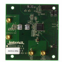
... Equivalent Circuits 0.535V ADC Evaluation Platform Intersil offers an ADC Evaluation platform which can be used to evaluate any of the KADxxxxx ADC family. The platform consists of a FPGA based data capture motherboard and a family of ADC daughtercards. This USB based platform allows a user to quickly evaluate the ADC’ ...
Page 32
The vias below the KAD5512P may be spaced further apart as shown on the evaluation board since low-power device. The via ...
Page 33
... REVISION 7/30/08 Rev 1 Initial Release of Production Data sheet 12/5/08 FN6807.0 Converted to intersil template. Assigned file number FN6807. Rev 0 - first release (as preliminary data sheet) with new file number. 12/23/08 FN6807.1 P1; revised Key Specs P2; added Part Marking column to Order Info P4; moved Thermal Resistance to Thermal Info table and added Theta JA Note 3 per packaging P4-6 ...
Page 34
... Accordingly, the reader is cautioned to verify that data sheets are current before placing orders. Information furnished by Intersil is believed to be accurate and reliable. However, no responsibility is assumed by Intersil or its subsidiaries for its use; nor for any infringements of patents or other rights of third parties which may result from its use. No license is granted by implication or otherwise under any patent or patent rights of Intersil or its subsidiaries ...
Page 35
Package Outline Drawing L48.7x7E 48 LEAD QUAD FLAT NO-LEAD PLASTIC PACKAGE Rev 1, 2/09 7.00 PIN 1 INDEX AREA 6 (4X) 0.15 TOP VIEW 6.80 Sq 5.60 Sq TYPICAL RECOMMENDED LAND PATTERN 35 KAD5512P Exp. DAP ...
Page 36
Package Outline Drawing L72.10x10D 72 LEAD QUAD FLAT NO-LEAD PLASTIC PACKAGE Rev 1, 11/08 10.00 PIN 1 INDEX AREA 6 (4X) 0.15 TOP VIEW 9.80 Sq 6.00 Sq TYPICAL RECOMMENDED LAND PATTERN 36 KAD5512P 10.00 37 ...