KDC2710CEVAL Intersil, KDC2710CEVAL Datasheet - Page 12
KDC2710CEVAL
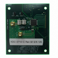
Manufacturer Part Number
KDC2710CEVAL
Description
DAUGHTER CARD FOR KAD2710
Manufacturer
Intersil
Series
FemtoCharge™r
Datasheets
1.KAD2710C-10Q68.pdf
(16 pages)
2.KMB-001LEVALZ.pdf
(7 pages)
3.KDC5514EVALZ.pdf
(9 pages)
Specifications of KDC2710CEVAL
Number Of Adc's
1
Number Of Bits
10
Sampling Rate (per Second)
275M
Data Interface
Parallel
Inputs Per Adc
1 Differential
Input Range
1.5 Vpp
Power (typ) @ Conditions
261mW @ 275MSPS
Voltage Supply Source
Single Supply
Operating Temperature
-40°C ~ 85°C
Utilized Ic / Part
KAD2710C-27, KMB001 Motherboard
For Use With
KMB001LEVAL - MOTHERBOARD FOR LVDS ADC CARD
Lead Free Status / RoHS Status
Lead free / RoHS Compliant


Functional Description
The KAD2710 is a ten bit, 275MSPS A/D converter in a
pipelined architecture. The input voltage is captured by a
sample and hold circuit and converted to a unit of charge.
Proprietary charge-domain techniques are used to compare
the input to a series of reference charges. These
comparisons determine the digital code for each input value.
The converter pipeline requires 24 sample clocks to produce
a result. Digital error correction is also applied, resulting in a
total latency of 28 clock cycles. This is evident to the user as
a latency between the start of a conversion and the data
being available on the digital outputs.
At power-up, a self-calibration is performed to minimize gain
and offset errors. The reset pin (RST) is held low internally at
power-up and will remain in that state until the calibration is
complete. The clock frequency should remain fixed during
this time.
Calibration accuracy is maintained for the sample rate at
which it is performed, and therefore should be repeated if the
clock frequency is changed by more than 10%. Recalibration
can be initiated via the RST pin, or power cycling, at any
time.
Reset
Recalibration of the ADC can be initiated at any time by
driving the RST pin low for a minimum of one clock cycle. An
open-drain driver is recommended.
The calibration sequence is initiated on the rising edge of
RST, as shown in Figure 21. The over-range output (OR) is
set high once RST is pulled low, and remains in that state
until calibration is complete. The OR output returns to
normal operation at that time, so it is important that the
analog input be within the converter’s full-scale range in
order to observe the transition. If the input is in an
over-range state the OR pin will stay high and it will not be
possible to detect the end of the calibration cycle.
While RST is low, the output clock (CLKOUT) stops toggling
and is set low. Normal operation of the output clock resumes
at the next input clock edge (CLKP/CLKN) after RST is
deasserted. At 275MSPS the nominal calibration time is
~240ms.
CLKOUTP
CLKN
CLKP
ORP
RST
FIGURE 21. CALIBRATION TIMING
Calibration Begins
12
Calibration Complete
Calibration Time
KAD2710C
Voltage Reference
The VREF pin is the reference voltage which sets the full-
scale input voltage for the chip. This pin requires a bypass
capacitor of 0.1uF at a minimum. The internally generated
bandgap reference voltage is provided by an on-chip voltage
buffer.buffer can sink or source up to 50µA externally.
An external voltage may be applied to this pin to provide a
more accurate reference than the internally generated
bandgap voltage, or to match the full-scale reference for
multiple KAD2710C chips.One option in the latter
configuration is to use one KAD2710C's internally generated
reference as the external reference voltage for the other
chips in the system. Additionally, an externally provided
reference can be changed from the nominal value to adjust
the full-scale input voltage within a limited range.
To select whether the full-scale reference is internally
generated or externally provided, the digital input VREFSEL
is set low for internal, or high for external.This pin has
internal pull-up.use the internally generated reference
VREFSEL can be tied directly to AVSS, and to use an
external reference VREFSEL can be left unconnected.
Analog Input
The ADC core contains a fully differential input (INP/INN) to
the sample and hold circuit. The ideal full-scale input voltage
is 1.50V, centered at the VCM voltage of 0.86V as shown in
Figure 22.
Best performance is obtained when the analog inputs are
driven differentially. The common-mode output voltage,
VCM, should be used to properly bias the inputs as shown in
Figures 23 and 24. An RF transformer will give the best
noise and distortion performance for wideband and/or high
intermediate frequency (IF) inputs. Two different transformer
input schemes are shown in Figures 23 and 24.
1.8
1.4
1.0
0.6
0.2
FIGURE 22. ANALOG INPUT RANGE
V
0.75V
INP
-0.75V
VCM
0.86V
December 5, 2008
INN
t
FN6814.0
Related parts for KDC2710CEVAL
Image
Part Number
Description
Manufacturer
Datasheet
Request
R

Part Number:
Description:
Intersil Corporation [CMOS Serial Controller Interface]
Manufacturer:
Intersil Corporation
Datasheet:
Part Number:
Description:
Manufacturer:
Intersil Corporation
Datasheet:
Part Number:
Description:
357-036-542-201 CARDEDGE 36POS DL .156 BLK LOPRO
Manufacturer:
Intersil Corporation
Datasheet:
Part Number:
Description:
1024-Word x 4-Bit LSI Static RAM
Manufacturer:
Intersil Corporation
Datasheet:
Part Number:
Description:
General Purpose NPN Transistor Arrays FN341.4
Manufacturer:
Intersil Corporation
Datasheet:
Part Number:
Description:
CMOS 16-Bit Microprocessor
Manufacturer:
Intersil Corporation
Datasheet:
Part Number:
Description:
Manufacturer:
Intersil Corporation
Datasheet:
Part Number:
Description:
Manufacturer:
Intersil Corporation
Datasheet:
Part Number:
Description:
Manufacturer:
Intersil Corporation
Datasheet:
Part Number:
Description:
Manufacturer:
Intersil Corporation
Datasheet:
Part Number:
Description:
CMOS 6-Bit Latch and Decoder Memory Interfaces
Manufacturer:
Intersil Corporation
Datasheet:
Part Number:
Description:
CA3046General Purpose NPN Transistor Arrays
Manufacturer:
Intersil Corporation
Datasheet:
Part Number:
Description:
Manufacturer:
Intersil Corporation
Datasheet:
Part Number:
Description:
TR909 DLC/FLC SLIC with Low Power Standby
Manufacturer:
Intersil Corporation
Datasheet:
Part Number:
Description:
Manufacturer:
Intersil Corporation
Datasheet: