MCP3221DM-PCTL Microchip Technology, MCP3221DM-PCTL Datasheet - Page 17
MCP3221DM-PCTL
Manufacturer Part Number
MCP3221DM-PCTL
Description
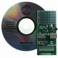
BOARD DEMO FOR PICTAIL MCP3221
Manufacturer
Microchip Technology
Series
PICtail™r
Type
A/Dr
Datasheets
1.MCP3221A5T-IOT.pdf
(28 pages)
2.MCP3221DM-PCTL.pdf
(20 pages)
3.MCP3221DM-PCTL.pdf
(20 pages)
Specifications of MCP3221DM-PCTL
Number Of Adc's
1
Number Of Bits
12
Sampling Rate (per Second)
22.3k
Data Interface
Serial
Inputs Per Adc
1 Single Ended
Voltage Supply Source
Single Supply
Operating Temperature
-40°C ~ 85°C
Utilized Ic / Part
MCP3221
Product
Data Conversion Development Tools
Resolution
12 bit
Interface Type
USB
Silicon Manufacturer
Microchip
Silicon Core Number
MCP3221
Kit Application Type
Data Converter
Application Sub Type
ADC
Silicon Family Name
PICtail
Kit Contents
Board Cables CD Docs
Rohs Compliant
Yes
For Use With/related Products
MCP3221
Lead Free Status / RoHS Status
Contains lead / RoHS non-compliant
Lead Free Status / RoHS Status
Lead free / RoHS Compliant, Contains lead / RoHS non-compliant
Available stocks
Company
Part Number
Manufacturer
Quantity
Price
Company:

Part Number:
MCP3221DM-PCTL
Manufacturer:
MICROCHIP
Quantity:
12 000


The input signal will initially be sampled with the first
falling edge of the clock following the transmission of a
logic-high R/W bit. Additionally, with the rising edge of
the SCL, the ADC will transmit an acknowledge bit
(ACK = 0). The master must release the data bus dur-
ing this clock pulse to allow the MCP3221 to pull the
line low (refer to Figure 5-3).
For consecutive samples, sampling begins on the fall-
ing edge of the LSB of the conversion result, which is
two bytes long. Refer to Figure 5-6 a for timing diagram.
FIGURE 5-5:
5.3.3
For consecutive samples, sampling begins on the fall-
ing edge of the LSB of the conversion result. See
Figure 5-6 for timing.
FIGURE 5-6:
© 2006 Microchip Technology Inc.
SDA
SCL
SDA
SCL
CONSECUTIVE CONVERSIONS
S
T
A
R
T
S
S
T
A
R
T
S
1
1
Device bits
1
1
Device bits
2
0
Executing a Conversion.
Continuous Conversion.
0
2
t
initiated here
ACQ
3
0
Address Byte
t
initiated here
ACQ
0
3
Address Byte
+ t
4
1
+ t
CONV
4
1 A2 A1 A0
Address bits
5
A
2
CONV
Address bits
5
is
6
A
1
is
6
A
7
0
7
W
R
8
/
W
R
8
/
9 10 11 12 13 14 15 16 17 18 19 20 21 22 23 24 25 26 27
A
C
K
A
C
K
9 10 11 12 13 14 15 16 17 18 19 20 21 22 23 24 25 26 27
0
0
0
0
Upper Data Byte
Upper Data Byte (n)
0
0
0
0
f
11 10
SAMP
D
11 10 9
D
5.3.2
Once the MCP3221 acknowledges the address byte,
the device will transmit four ‘0’ bits followed by the upper
four data bits of the conversion. The master device will
then acknowledge this byte with an ACK = Low. With the
following 8 clock pulses, the MCP3221 will transmit the
lower eight data bits from the conversion. The master
then sends an ACK = high, indicating to the MCP3221
that no more data is requested. The master can then
send a stop bit to end the transmission.
D
= 22.3 ksps (f
D
D
9
D
D
8
D
8
A
C
K
READING THE CONVERSION DATA
CLK
A
C
K
D
7
= 400 kHz)
D
7
D
6
D
6
Lower Data Byte
Lower Data Byte (n)
D
5
t
initiated here
ACQ
D
5
D
4
+ t
D
4
D
3
CONV
D
3
MCP3221
D
2
is
D
2
D
1
D
1
DS21732C-page 17
D
0
D
0
N
A
K
A
C
K
S
T
O
P
P
28
0
Related parts for MCP3221DM-PCTL
Image
Part Number
Description
Manufacturer
Datasheet
Request
R

Part Number:
Description:
Manufacturer:
Microchip Technology Inc.
Datasheet:
Part Number:
Description:
Manufacturer:
Microchip Technology Inc.
Datasheet:
Part Number:
Description:
Manufacturer:
Microchip Technology Inc.
Datasheet:
Part Number:
Description:
Manufacturer:
Microchip Technology Inc.
Datasheet:
Part Number:
Description:
Manufacturer:
Microchip Technology Inc.
Datasheet:
Part Number:
Description:
Manufacturer:
Microchip Technology Inc.
Datasheet:
Part Number:
Description:
Manufacturer:
Microchip Technology Inc.
Datasheet:
Part Number:
Description:
Manufacturer:
Microchip Technology Inc.
Datasheet: