MCP3221DM-PCTL Microchip Technology, MCP3221DM-PCTL Datasheet - Page 18
MCP3221DM-PCTL
Manufacturer Part Number
MCP3221DM-PCTL
Description
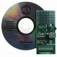
BOARD DEMO FOR PICTAIL MCP3221
Manufacturer
Microchip Technology
Series
PICtail™r
Type
A/Dr
Datasheets
1.MCP3221A5T-IOT.pdf
(28 pages)
2.MCP3221DM-PCTL.pdf
(20 pages)
3.MCP3221DM-PCTL.pdf
(20 pages)
Specifications of MCP3221DM-PCTL
Number Of Adc's
1
Number Of Bits
12
Sampling Rate (per Second)
22.3k
Data Interface
Serial
Inputs Per Adc
1 Single Ended
Voltage Supply Source
Single Supply
Operating Temperature
-40°C ~ 85°C
Utilized Ic / Part
MCP3221
Product
Data Conversion Development Tools
Resolution
12 bit
Interface Type
USB
Silicon Manufacturer
Microchip
Silicon Core Number
MCP3221
Kit Application Type
Data Converter
Application Sub Type
ADC
Silicon Family Name
PICtail
Kit Contents
Board Cables CD Docs
Rohs Compliant
Yes
For Use With/related Products
MCP3221
Lead Free Status / RoHS Status
Contains lead / RoHS non-compliant
Lead Free Status / RoHS Status
Lead free / RoHS Compliant, Contains lead / RoHS non-compliant
Available stocks
Company
Part Number
Manufacturer
Quantity
Price
Company:

Part Number:
MCP3221DM-PCTL
Manufacturer:
MICROCHIP
Quantity:
12 000


MCP3221
6.0
6.1
The MCP3221 has a single-ended analog input (AIN).
For proper conversion results, the voltage at the AIN
pin must be kept between
has no offset error, gain error, INL or DNL errors, and
the voltage level of AIN is equal to or less than
V
tionally, if the voltage at AIN is equal to or greater than
V
FIGURE 6-1:
6.2
The I
resistors connected to the SDA and SCL lines. This
configuration is shown in Figure 6-2.
FIGURE 6-2:
Bus.
DS21732C-page 18
SS
DD
Legend
+ 1/2 LSB, the resultant code will be 000h. Addi-
- 1.5 LSB, the output code will be FFFh.
I
C
2
V
LEAKAGE
C bus is an open-collector bus, requiring pull-up
A
SAMPLE
R
PU
APPLICATIONS INFORMATION
Driving the Analog Input
Connecting to the I
R
C
R
A
SS
VA
PIN
SS
V
R
is typically: 10 kΩ for f
SS
IN
T
S
A
R
=
=
=
=
=
=
=
=
=
IN
PU
signal source
source impedance
analog input pad
analog input pin capacitance
threshold voltage
leakage current at the pin
due to various junctions
sampling switch
sampling switch resistor
sample/hold capacitance
V
Analog Input Model, A
Pull-up Resistors on I
R
DD
2 kΩ for f
PU
V
SS
SDA
SCL
MCP3221
7 pF
C
and
PIN
SCL
SCL
2
V
C Bus
A
DD
IN
V
= 100 kHz
= 400 kHz
. If the converter
DD
V
V
T
T
Analog
Input
Signal
= 0.6V
= 0.6V
2
IN
C
.
I
±1 nA
LEAKAGE
The analog input model is shown in Figure 6-1. In this
diagram, the source impedance (R
nal sampling switch (R
the time required to charge the capacitor (C
Consequently, a larger source impedance increases
the offset error, gain error and integral linearity errors of
the conversion. Ideally, the impedance of the signal
source should be near zero. This is achievable with an
operational amplifier, such as the MCP6022, which has
a closed-loop output impedance of tens of ohms.
The number of devices connected to the bus is limited
only by the maximum bus capacitance of 400 pF. A
possible configuration using multiple devices is shown
in Figure 6-3.
FIGURE 6-3:
Bus.
Microcontroller
PIC16F876
12-bit ADC
MCP3221
SS
Sampling
Switch
R
S
= 1 kΩ
Multiple Devices on I
S
SDA SCL
© 2006 Microchip Technology Inc.
) impedance, directly affecting
V
SS
C
= DAC capacitance
= 20 pF
SAMPLE
SS
Temperature
EEPROM
24LC01
) adds to the inter-
Sensor
TC74
SAMPLE
2
C™
).
Related parts for MCP3221DM-PCTL
Image
Part Number
Description
Manufacturer
Datasheet
Request
R

Part Number:
Description:
Manufacturer:
Microchip Technology Inc.
Datasheet:
Part Number:
Description:
Manufacturer:
Microchip Technology Inc.
Datasheet:
Part Number:
Description:
Manufacturer:
Microchip Technology Inc.
Datasheet:
Part Number:
Description:
Manufacturer:
Microchip Technology Inc.
Datasheet:
Part Number:
Description:
Manufacturer:
Microchip Technology Inc.
Datasheet:
Part Number:
Description:
Manufacturer:
Microchip Technology Inc.
Datasheet:
Part Number:
Description:
Manufacturer:
Microchip Technology Inc.
Datasheet:
Part Number:
Description:
Manufacturer:
Microchip Technology Inc.
Datasheet: