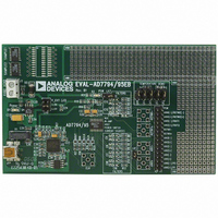
EVAL-AD7794EBZ Analog Devices Inc, EVAL-AD7794EBZ Datasheet - Page 11
EVAL-AD7794EBZ
Manufacturer Part Number
EVAL-AD7794EBZ
Description
BOARD EVALUATION FOR AD7794
Manufacturer
Analog Devices Inc
Specifications of EVAL-AD7794EBZ
Number Of Adc's
1
Number Of Bits
24
Sampling Rate (per Second)
470
Data Interface
SPI™, QSPI™, MICROWIRE™, and DSP
Inputs Per Adc
6 Differential
Input Range
±VREF/gain
Power (typ) @ Conditions
2.5mW @ 470SPS
Voltage Supply Source
Analog and Digital
Operating Temperature
-40°C ~ 105°C
Utilized Ic / Part
AD7794
Lead Free Status / RoHS Status
Lead free / RoHS Compliant


PIN CONFIGURATION AND FUNCTION DESCRIPTIONS
Table 4. Pin Function Descriptions
Pin No.
1
2
3
4
5
6
7
8
9
10
11
12
13
14
15
16
17
Mnemonic
SCLK
CLK
CS
NC
AIN6(+)/P1
AIN6(−)/P2
AIN1(+)
AIN1(−)
AIN2(+)
AIN2(−)
AIN3(+)
AIN3(−)
REFIN1(+)
REFIN1(−)
AIN5(+)/IOUT2
AIN5(−)/IOUT1
AIN4(+)/REFIN2(+)
Description
Serial Clock Input. This serial clock input is for data transfers to and from the ADC. The SCLK has a Schmitt-
triggered input, making the interface suitable for opto-isolated applications. The serial clock can be
continuous with all data transmitted in a continuous train of pulses. Alternatively, it can be a noncontinuous
clock with the information being transmitted to or from the ADC in smaller batches of data.
Clock In/Clock Out. The internal clock can be made available at this pin. Alternatively, the internal clock can
be disabled, and the ADC can be driven by an external clock. This allows several ADCs to be driven from a
common clock, allowing simultaneous conversions to be performed.
Chip Select Input. This is an active low logic input used to select the ADC. CS can be used to select the ADC in
systems with more than one device on the serial bus or as a frame synchronization signal in communicating
with the device. CS can be hardwired low, allowing the ADC to operate in 3-wire mode with SCLK, DIN, and
DOUT used to interface with the device.
No Connect.
Analog Input/Digital Output Pin. AIN6(+) is the positive terminal of the differential analog input pair,
AIN6(+)/AIN6(−). This pin can also function as a general-purpose output bit referenced between AV
Analog Input/Digital Output Pin. AIN6(−) is the negative terminal of the differential analog input pair,
AIN6(+)/AIN6(−). This pin can also function as a general-purpose output bit referenced between AV
Analog Input. AIN1(+) is the positive terminal of the differential analog input pair, AIN1(+)/AIN1(−).
Analog Input. AIN1(−) is the negative terminal of the differential analog input pair, AIN1(+)/AIN1(−).
Analog Input. AIN2(+) is the positive terminal of the differential analog input pair, AIN2(+)/AIN2(−).
Analog Input. AIN2(−) is the negative terminal of the differential analog input pair, AIN2(+)/AIN2(−).
Analog Input. AIN3(+) is the positive terminal of the differential analog input pair, AIN3(+)/AIN3(−).
Analog Input. AIN3(−) is the negative terminal of the differential analog input pair, AIN3(+)/AIN3(−).
Positive Reference Input. An external reference can be applied between REFIN1(+) and REFIN1(−). REFIN1(+)
can lie anywhere between AV
2.5 V, but the part functions with a reference from 0.1 V to AV
Negative Reference Input. This reference input can lie anywhere between GND and AV
Analog Input/Output of Internal Excitation Current Source. AIN5(+) is the positive terminal of the differential
analog input pair AIN5(+)/AIN5(−). Alternatively, the internal excitation current source can be made available at
this pin and is programmable so that the current can be 10 μA, 210 μA, or 1 mA. Either IEXC1 or IEXC2 can be
switched to this output.
Analog Input/Output of Internal Excitation Current Source. AIN5(−) is the negative terminal of the
differential analog input pair, AIN5(+)/AIN5(−). Alternatively, the internal excitation current source can be
made available at this pin and is programmable so that the current can be 10 μA, 210 μA, or 1 mA. Either
IEXC1 or IEXC2 can be switched to this output.
Analog Input/Positive Reference Input. AIN4(+) is the positive terminal of the differential analog input pair
AIN4(+)/AIN4(−). This pin also functions as a positive reference input for REFIN2. REFIN2(+) can lie anywhere
between AV
functions with a reference from 0.1 V to AV
DD
and GND + 0.1 V. The nominal reference voltage (REFIN2(+) to REFIN2(−)) is 2.5 V, but the part
AIN6(+)/P1
AIN6(–)/P2
AIN1(+)
AIN2(+)
AIN3(+)
AIN1(–)
AIN2(–)
AIN3(–)
SCLK
CLK
NC
CS
Figure 5. Pin Configuration
10
11
12
1
2
3
4
5
6
7
8
9
NC = NO CONNECT
Rev. D | Page 11 of 36
DD
(Not to Scale)
AD7794/
AD7795
TOP VIEW
and GND + 0.1 V. The nominal reference voltage, (REFIN1(+) − REFIN1(−)), is
24
23
22
21
20
19
18
17
16
15
14
13
DD
DIN
DOUT/RDY
DV
AV
GND
PSW
AIN4(–)/REFIN2(–)
AIN4(+)/REFIN2(+)
AIN5(–)/IOUT1
AIN5(+)/IOUT2
REFIN1(–)
REFIN1(+)
.
DD
DD
DD
.
AD7794/AD7795
DD
− 0.1 V.
DD
DD
and GND.
and GND.
Related parts for EVAL-AD7794EBZ
Image
Part Number
Description
Manufacturer
Datasheet
Request
R


Part Number:
Description:
BOARD EVAL FOR SI270X-A
Manufacturer:
Silicon Laboratories Inc
Datasheet:

Part Number:
Description:
BUCK CONV REF DESIGN KIT IP1201
Manufacturer:
International Rectifier
Datasheet:
Part Number:
Description:
BOARD DEMO SYNC DUAL BUCK CNVTER
Manufacturer:
International Rectifier
Datasheet:
Part Number:
Description:
BOARD DEMO SYNC BUCK CONVETER
Manufacturer:
International Rectifier
Datasheet:

Part Number:
Description:
EVALBOARD/EB Omnidirectional microphone - Analog
Manufacturer:
Analog Devices
Datasheet:
Part Number:
Description:
EVALBOARD/EB Omnidirectional microphone - Analog
Manufacturer:
Analog Devices
Datasheet:


Part Number:
Description:
BOARD EVAL LED DRIVER LT3756
Manufacturer:
Linear Technology
Datasheet:

Part Number:
Description:
BOARD EVAL FOR AD7741/7742
Manufacturer:
Analog Devices Inc
Datasheet:

Part Number:
Description:
±1.7g Dual-Axis IMEMS Accelerometer Evaluation Board
Manufacturer:
Analog Devices Inc
Datasheet:

Part Number:
Description:
IC MULTIPLIER ANALOG 8-SOIC T/R
Manufacturer:
Analog Devices Inc
Datasheet:

Part Number:
Description:
IC ANALOG MULTIPLIER 8-DIP
Manufacturer:
Analog Devices Inc
Datasheet:
Part Number:
Description:
IC ANALOG MULTIPLIER 8-SOIC
Manufacturer:
Analog Devices Inc
Datasheet:
Part Number:
Description:
IC ANALOG MULTIPLIER 8-DIP
Manufacturer:
Analog Devices Inc
Datasheet: