EVAL-AD7794EBZ Analog Devices Inc, EVAL-AD7794EBZ Datasheet - Page 34
EVAL-AD7794EBZ
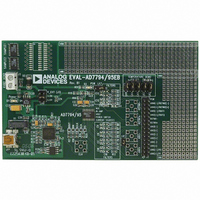
Manufacturer Part Number
EVAL-AD7794EBZ
Description
BOARD EVALUATION FOR AD7794
Manufacturer
Analog Devices Inc
Specifications of EVAL-AD7794EBZ
Number Of Adc's
1
Number Of Bits
24
Sampling Rate (per Second)
470
Data Interface
SPI™, QSPI™, MICROWIRE™, and DSP
Inputs Per Adc
6 Differential
Input Range
±VREF/gain
Power (typ) @ Conditions
2.5mW @ 470SPS
Voltage Supply Source
Analog and Digital
Operating Temperature
-40°C ~ 105°C
Utilized Ic / Part
AD7794
Lead Free Status / RoHS Status
Lead free / RoHS Compliant


AD7794/AD7795
one conversion cycle when chop is disabled. For higher gains,
four conversion cycles are required to perform the full-scale
calibration when chop is enabled, and two conversion cycles
when chop is disabled. DOUT/ RDY goes high when the
calibration is initiated and returns low when the calibration is
complete. The ADC is placed in idle mode following a cali-
bration. The measured full-scale coefficient is placed in the full-
scale register of the selected channel. Internal full-scale
calibrations cannot be performed when the gain equals 128.
With this gain setting, a system full-scale calibration can be
performed. A full-scale calibration is required each time the
gain of a channel is changed to minimize the full-scale error.
An internal full-scale calibration can be performed at specified
update rates only. For gains of 1, 2, and 4, an internal full-scale
calibration can be performed at any update rate. However, for
higher gains, internal full-scale calibrations can be performed
only when the update rate is less than or equal to 16.7 Hz, 33.3 Hz,
and 50 Hz. However, the full-scale error does not vary with
update rate, so a calibration at one update is valid for all update
rates (assuming the gain or reference source is not changed).
A system full-scale calibration takes two conversion cycles to
complete, irrespective of the gain setting when chop is enabled
and one conversion cycle when chop is disabled. A system full-
scale calibration can be performed at all gains and all update
rates. With chop disabled, the offset calibration (internal or
system offset) should be performed before the system full-scale
calibration is initiated.
GROUNDING AND LAYOUT
Because the analog inputs and reference inputs of the ADC are
differential, most of the voltages in the analog modulator are
common-mode voltages. The excellent common-mode
rejection of the part removes common-mode noise on these
inputs. The digital filter provides rejection of broadband noise
on the power supply, except at integer multiples of the
modulator sampling frequency. The digital filter also removes
noise from the analog and reference inputs, provided that these
noise sources do not saturate the analog modulator. As a result,
the AD7794/AD7795 are more immune to noise interference
than conventional high resolution converters. However, because
the resolution of the AD7794/AD7795 is so high, and the noise
Rev. D | Page 34 of 36
levels from the AD7794/AD7795 are so low, care must be taken
with regard to grounding and layout.
The printed circuit board that houses the AD7794/AD7795
should be designed so that the analog and digital sections are
separated and confined to certain areas of the board. A minimum
etch technique is generally best for ground planes because it
gives the best shielding.
It is recommended that the GND pin of the AD7794/AD7795
be tied to the AGND plane of the system. In any layout, it is
important that the user keep in mind the flow of currents in the
system, ensuring that the return paths for all currents are as
close as possible to the paths the currents took to reach their
destinations. Avoid forcing digital currents to flow through the
AGND sections of the layout.
The ground plane of the AD7794/AD7795 should be allowed to
run under the AD7794/AD7795 to prevent noise coupling. The
power supply lines to the AD7794/AD7795 should use as wide a
trace as possible to provide low impedance paths and reduce the
effects of glitches on the power supply line. Fast switching
signals, such as clocks, should be shielded with digital ground
to avoid radiating noise to other sections of the board. In
addition, clock signals should never be run near the analog
inputs. Avoid crossover of digital and analog signals. Traces on
opposite sides of the board should run at right angles to each
other. This reduces the effects of feedthrough through the
board. A microstrip technique is the best, but it is not always
possible with a double-sided board. In this technique, the
component side of the board is dedicated to ground planes,
while signals are placed on the solder side.
Good decoupling is important when using high resolution
ADCs. AV
parallel with 0.1 μF capacitors to GND. DV
decoupled with 10 μF tantalum in parallel with 0.1 μF
capacitors to the system’s DGND plane, with the system’s
AGND to DGND connection being close to the
AD7794/AD7795. To achieve the best from these decoupling
components, they should be placed as close as possible to the
device, ideally right up against the device. All logic chips should
be decoupled with 0.1 μF ceramic capacitors to DGND.
DD
should be decoupled with 10 μF tantalum in
DD
should be
Related parts for EVAL-AD7794EBZ
Image
Part Number
Description
Manufacturer
Datasheet
Request
R


Part Number:
Description:
BOARD EVAL FOR SI270X-A
Manufacturer:
Silicon Laboratories Inc
Datasheet:

Part Number:
Description:
BUCK CONV REF DESIGN KIT IP1201
Manufacturer:
International Rectifier
Datasheet:
Part Number:
Description:
BOARD DEMO SYNC DUAL BUCK CNVTER
Manufacturer:
International Rectifier
Datasheet:
Part Number:
Description:
BOARD DEMO SYNC BUCK CONVETER
Manufacturer:
International Rectifier
Datasheet:

Part Number:
Description:
EVALBOARD/EB Omnidirectional microphone - Analog
Manufacturer:
Analog Devices
Datasheet:
Part Number:
Description:
EVALBOARD/EB Omnidirectional microphone - Analog
Manufacturer:
Analog Devices
Datasheet:


Part Number:
Description:
BOARD EVAL LED DRIVER LT3756
Manufacturer:
Linear Technology
Datasheet:

Part Number:
Description:
BOARD EVAL FOR AD7741/7742
Manufacturer:
Analog Devices Inc
Datasheet:

Part Number:
Description:
±1.7g Dual-Axis IMEMS Accelerometer Evaluation Board
Manufacturer:
Analog Devices Inc
Datasheet:

Part Number:
Description:
IC MULTIPLIER ANALOG 8-SOIC T/R
Manufacturer:
Analog Devices Inc
Datasheet:

Part Number:
Description:
IC ANALOG MULTIPLIER 8-DIP
Manufacturer:
Analog Devices Inc
Datasheet:
Part Number:
Description:
IC ANALOG MULTIPLIER 8-SOIC
Manufacturer:
Analog Devices Inc
Datasheet:
Part Number:
Description:
IC ANALOG MULTIPLIER 8-DIP
Manufacturer:
Analog Devices Inc
Datasheet: