CDB5560 Cirrus Logic Inc, CDB5560 Datasheet - Page 19
CDB5560
Manufacturer Part Number
CDB5560
Description
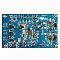
DEV BOARD FOR CS5560 W/MUX
Manufacturer
Cirrus Logic Inc
Type
A/Dr
Specifications of CDB5560
Number Of Adc's
1
Number Of Bits
24
Sampling Rate (per Second)
50k
Data Interface
Serial
Inputs Per Adc
1 Differential
Input Range
±3 V
Power (typ) @ Conditions
90mW @ 2.5 V
Voltage Supply Source
Dual ±
Operating Temperature
-40°C ~ 85°C
Utilized Ic / Part
CS5560
Product
Data Conversion Development Tools
Conversion Rate
50 KSPS
Resolution
24 bit
Maximum Clock Frequency
16 MHz
Interface Type
SPI
Supply Voltage (max)
3.3 V
Supply Voltage (min)
- 2.5 V
For Use With/related Products
CS5560
Lead Free Status / RoHS Status
Contains lead / RoHS non-compliant
Lead Free Status / RoHS Status
Lead free / RoHS Compliant, Contains lead / RoHS non-compliant
Other names
598-1273
CDB5560-1
CDB5560-1


5/4/09
CS5560
3.7 AIN & VREF Sampling Structures
The CS5560 uses on-chip buffers on the AIN+, AIN-, and the VREF+ inputs. Buffers provide much higher
input impedance and therefore reduce the amount of drive current required from an external source. This
helps minimize errors.
The Buffer Enable (BUFEN) pin determines if the on-chip buffers are used or not. If the BUFEN pin is
connected to the V1+ supply, the buffers will be enabled. If the BUFEN pin is connected to the V1- pin,
the buffers are off. The converter will consume about 30 mW less power when the buffers are off, but the
input impedances of AIN+, AIN- and VREF+ will be significantly less than with the buffers enabled.
3.8 Converter Performance
The CS5560 achieves excellent differential nonlinearity (DNL) as shown in Figure 8. Figure 8 illustrates
the code widths on the typical scale of ±1 LSB and on a zoomed scale of ±0.2 LSB.
(Zoom View)
Figure 8. CS5560 DNL Plot
DS713PP2
19
Related parts for CDB5560
Image
Part Number
Description
Manufacturer
Datasheet
Request
R

Part Number:
Description:
Development Kit
Manufacturer:
Cirrus Logic Inc
Datasheet:
Part Number:
Description:
Development Kit
Manufacturer:
Cirrus Logic Inc
Datasheet:


Part Number:
Description:
High-efficiency PFC + Fluorescent Lamp Driver Reference Design
Manufacturer:
Cirrus Logic Inc
Datasheet:
Part Number:
Description:
Development Kit
Manufacturer:
Cirrus Logic Inc
Datasheet:
Part Number:
Description:
Development Kit
Manufacturer:
Cirrus Logic Inc
Datasheet:

Part Number:
Description:
Development Kit
Manufacturer:
Cirrus Logic Inc
Datasheet:
Part Number:
Description:
Development Kit
Manufacturer:
Cirrus Logic Inc
Datasheet:
Part Number:
Description:
Development Kit
Manufacturer:
Cirrus Logic Inc
Datasheet:
Part Number:
Description:
Development Kit
Manufacturer:
Cirrus Logic Inc
Datasheet:

Part Number:
Description:
EVALUATION BOARD FOR CS8427
Manufacturer:
Cirrus Logic Inc
Datasheet:

Part Number:
Description:
BOARD EVAL FOR CS8416 RCVR
Manufacturer:
Cirrus Logic Inc
Datasheet:

Part Number:
Description:
EVALUATION BOARD FOR CS8420
Manufacturer:
Cirrus Logic Inc
Datasheet:

Part Number:
Description:
KIT DEVELOPMENT EP9315 ARM9
Manufacturer:
Cirrus Logic Inc
Datasheet:

Part Number:
Description:
KIT DEVELOPMENT EP9302 ARM9
Manufacturer:
Cirrus Logic Inc
Datasheet: