EVAL-AD7708EBZ Analog Devices Inc, EVAL-AD7708EBZ Datasheet - Page 3
EVAL-AD7708EBZ
Manufacturer Part Number
EVAL-AD7708EBZ
Description
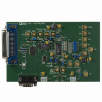
BOARD EVAL FOR AD7708
Manufacturer
Analog Devices Inc
Specifications of EVAL-AD7708EBZ
Number Of Adc's
1
Number Of Bits
16
Sampling Rate (per Second)
1.37k
Data Interface
Serial
Inputs Per Adc
8 Single or 4 Differential
Input Range
±2.5 V
Power (typ) @ Conditions
3.84mW @ 3 V
Voltage Supply Source
Analog and Digital
Operating Temperature
-40°C ~ 85°C
Utilized Ic / Part
AD7708
Lead Free Status / RoHS Status
Lead free / RoHS Compliant
Other names
EVAL-AD7708EB
EVAL-AD7708EB
EVAL-AD7708EB


LK12
LK13
LK14&15
EVALUATION BOARD INTERFACING
Interfacing to the evaluation board is via either a 9-way d-type connector, J4 or a 36-way centronics connector,
J1. The pin-out for the J4 connector is shown in Fig. 2 and its pin designations are given in Table 2. The pin-
out for the J1 connector is shown in Fig. 3 and its pin designations are given in Table 3.
J1 is used to connect the evaluation board to the parallel (printer) port of a PC. Connection is via a standard printer
cable. J4 is used to connect the evaluation to any other system. The evaluation board should be powered up before
a cable is connected to either of these connectors.
Table 2.:
1 S C L K
2
3
4
5 D I N
6 D G N D
7 D O U T
8 DV
9 N C
Note
descriptions.
Table 3: 36-Way Connector Pin Description
1
2
3
1
An explanation of the AD7708 functions mentioned here is given in Table 3 below as part of the J1 pin
DD
N C
D I N
A
A
B
Serial Clock. The signal on this pin is buffered before being applied to the SCLK pin of the
AD7708.
Logic output. This is a buffered version of the signal on the AD7708
Chip Select. The signal on this pin is buffered before being applied to the
Reset Input. Data applied to this pin is buffered before being applied to the AD7708
Serial Data Input. Data applied to this pin is buffered before being applied to the AD7708 DIN
pin.
Ground reference point for the digital circuitry. Connects to the DGND plane on the Evaluation
board.
Serial Data Output. This is a buffered version of the signal on the AD7708 DOUT pin.
Digital Supply Voltage. If no voltage is applied to the board's DV
applied to this pin will supply the DV
Not Connected.
J4 Pin Description
No Connect. This pin is not connected on the evaluation board.
Serial Data Input. Data applied to this pin is buffered before being applied to the
AD7708 DIN pin. Serial Data Input with serial data being written to the input shift
register on the part. Data from this input shift register is transferred to the calibration
or control registers, depending on the register selection bits of the Communications
Register.
Reset Input. The signal on this pin is buffered before being applied to the
of the AD7708.
logic, calibration coefficients, digital filter and analog modulator of the part to power-
on status.
The on-board reference (U6) provides the reference voltage for the REFIN1(+) input
of the AD7708.
This connects the REFIN1(-) input of the AD7708 to AGND.
Both links in position B to select the on-board crystal as the master clock for the
AD7708.
Fig. 2: Pin Configuration for the 9-Way D-Type Connector, J4.
1
1
6
is an active low input which resets the control logic, interface
2
DD
7
- 3 -
for the digital buffers.
3
8
4
9
5
EVAL-AD7708-EB
DD
input terminal then the voltage
pin
pin on the AD7708.
pin.
pin
Rev. O
Related parts for EVAL-AD7708EBZ
Image
Part Number
Description
Manufacturer
Datasheet
Request
R


Part Number:
Description:
BOARD EVAL FOR SI270X-A
Manufacturer:
Silicon Laboratories Inc
Datasheet:

Part Number:
Description:
BUCK CONV REF DESIGN KIT IP1201
Manufacturer:
International Rectifier
Datasheet:
Part Number:
Description:
BOARD DEMO SYNC DUAL BUCK CNVTER
Manufacturer:
International Rectifier
Datasheet:
Part Number:
Description:
BOARD DEMO SYNC BUCK CONVETER
Manufacturer:
International Rectifier
Datasheet:

Part Number:
Description:
EVALBOARD/EB Omnidirectional microphone - Analog
Manufacturer:
Analog Devices
Datasheet:
Part Number:
Description:
EVALBOARD/EB Omnidirectional microphone - Analog
Manufacturer:
Analog Devices
Datasheet:


Part Number:
Description:
BOARD EVAL LED DRIVER LT3756
Manufacturer:
Linear Technology
Datasheet:

Part Number:
Description:
BOARD EVAL FOR AD7741/7742
Manufacturer:
Analog Devices Inc
Datasheet:

Part Number:
Description:
±1.7g Dual-Axis IMEMS Accelerometer Evaluation Board
Manufacturer:
Analog Devices Inc
Datasheet:

Part Number:
Description:
IC MULTIPLIER ANALOG 8-SOIC T/R
Manufacturer:
Analog Devices Inc
Datasheet:

Part Number:
Description:
IC ANALOG MULTIPLIER 8-DIP
Manufacturer:
Analog Devices Inc
Datasheet:
Part Number:
Description:
IC ANALOG MULTIPLIER 8-SOIC
Manufacturer:
Analog Devices Inc
Datasheet:
Part Number:
Description:
IC ANALOG MULTIPLIER 8-DIP
Manufacturer:
Analog Devices Inc
Datasheet: