EVAL-AD7708EBZ Analog Devices Inc, EVAL-AD7708EBZ Datasheet - Page 4
EVAL-AD7708EBZ
Manufacturer Part Number
EVAL-AD7708EBZ
Description
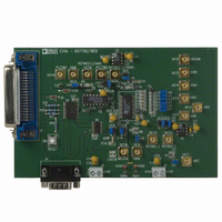
BOARD EVAL FOR AD7708
Manufacturer
Analog Devices Inc
Specifications of EVAL-AD7708EBZ
Number Of Adc's
1
Number Of Bits
16
Sampling Rate (per Second)
1.37k
Data Interface
Serial
Inputs Per Adc
8 Single or 4 Differential
Input Range
±2.5 V
Power (typ) @ Conditions
3.84mW @ 3 V
Voltage Supply Source
Analog and Digital
Operating Temperature
-40°C ~ 85°C
Utilized Ic / Part
AD7708
Lead Free Status / RoHS Status
Lead free / RoHS Compliant
Other names
EVAL-AD7708EB
EVAL-AD7708EB
EVAL-AD7708EB


EVAL-AD7708-EB
4
5
6
7-8
9
10
11-12
13
14-18
19-30
31-36
S O C K E T S
There are eighteen sockets relevant to the operation of the AD7708 on this evaluation board. The functions of
these sockets are outlined in Table 4.
Table 4. Socket Functions
Socket
J4
J1
S C L K
N C
DV
N C
D O U T
N C
D G N D
N C
Function
9-way D-Type connector used to interface to other systems.
36-way centronics connector used to interface to PC via parallel printer port.
DD
18
36
Chip Select. The signal on this pin is buffered before being applied to the
AD7708.
hard-wired low, the AD7708 can operate in its three-wire interface mode with SCLK,
DIN and DOUT used to interface to the device.
systems with more than one device on the serial bus or as a frame synchronization signal
in communicating with the AD7708.
Serial Clock. The signal on this pin is buffered before being applied to the SCLK pin
of the AD7708. An external serial clock is applied to this input to read/write serial data
from/to the AD7708. This serial clock can be continuous with all data transmitted in
a continuous train of pulses. Alternatively, it can be non-continuous with the information
being transmitted to the AD7708 in smaller batches of data.
Logic Input. The signal on this pin is buffered before being applied to the
of the AD7708. The
modulators across a number of AD7708s. While
filter, the filter control logic and the calibration control logic are held in a reset state.
No Connect. These pins are not connected on the evaluation board.
Digital Supply Voltage. This provides the supply voltage for the buffer chips, U3-U5,
which buffer the signals between the AD7708 and J1/J4.
Logic output. This is a buffered version of the signal on the AD7708
low on this output indicates that either the Main ADC or Auxiliary ADC has valid data
in their data register. The
of a full output word. If data is not read
indicating to the user that a read operation should not be initiated. The
returns low after the completion of a calibration cycle. The
NOR of the RDY0 and RDY1 bits in the Status register. If one of the ADCs is disabled
the
the mode bits are written to enabling a new conversion or calibration.
No Connect. These pins are not connected on the evaluation board.
Serial Data Output. This is a buffered version of the signal on the AD7708 DOUT pin.
Serial Data Output with serial data obtained from the output shift register on the
AD7708. The output shift register can contain information from of the on-chip registers
depending on the register selection bits of the Communications Register.
No Connect. These pins are not connected on the evaluation board.
Ground reference point for digital circuitry. Connects to the DGND plane on the
evaluation board.
No Connect. These pins are not connected on the evaluation board.
Fig. 3:
pin reflects the active ADC.
36-way Centronics (SKT2) Pin Configuration
is an active low Logic Input used to select the AD7708. With this input
input allows for synchronisation of the digital filters and
- 4 -
pin will return high upon completion of a read operation
does not return high aftera calibration until
will return high prior to the next update
can be used to select the device in
is low, the nodes of the digital
19
1
pin is effectively the
pin. A logic
pin of the
pin also
pin
Rev. O
Related parts for EVAL-AD7708EBZ
Image
Part Number
Description
Manufacturer
Datasheet
Request
R


Part Number:
Description:
BOARD EVAL FOR SI270X-A
Manufacturer:
Silicon Laboratories Inc
Datasheet:

Part Number:
Description:
BUCK CONV REF DESIGN KIT IP1201
Manufacturer:
International Rectifier
Datasheet:
Part Number:
Description:
BOARD DEMO SYNC DUAL BUCK CNVTER
Manufacturer:
International Rectifier
Datasheet:
Part Number:
Description:
BOARD DEMO SYNC BUCK CONVETER
Manufacturer:
International Rectifier
Datasheet:

Part Number:
Description:
EVALBOARD/EB Omnidirectional microphone - Analog
Manufacturer:
Analog Devices
Datasheet:
Part Number:
Description:
EVALBOARD/EB Omnidirectional microphone - Analog
Manufacturer:
Analog Devices
Datasheet:


Part Number:
Description:
BOARD EVAL LED DRIVER LT3756
Manufacturer:
Linear Technology
Datasheet:

Part Number:
Description:
BOARD EVAL FOR AD7741/7742
Manufacturer:
Analog Devices Inc
Datasheet:

Part Number:
Description:
±1.7g Dual-Axis IMEMS Accelerometer Evaluation Board
Manufacturer:
Analog Devices Inc
Datasheet:

Part Number:
Description:
IC MULTIPLIER ANALOG 8-SOIC T/R
Manufacturer:
Analog Devices Inc
Datasheet:

Part Number:
Description:
IC ANALOG MULTIPLIER 8-DIP
Manufacturer:
Analog Devices Inc
Datasheet:
Part Number:
Description:
IC ANALOG MULTIPLIER 8-SOIC
Manufacturer:
Analog Devices Inc
Datasheet:
Part Number:
Description:
IC ANALOG MULTIPLIER 8-DIP
Manufacturer:
Analog Devices Inc
Datasheet: