EVAL-AD7731EBZ Analog Devices Inc, EVAL-AD7731EBZ Datasheet - Page 2
EVAL-AD7731EBZ
Manufacturer Part Number
EVAL-AD7731EBZ
Description
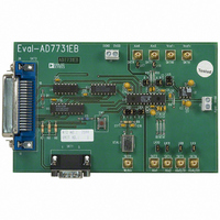
BOARD EVALUATION FOR AD7731
Manufacturer
Analog Devices Inc
Datasheets
1.AD7731BRUZ.pdf
(44 pages)
2.EVAL-AD7731EBZ.pdf
(11 pages)
3.EVAL-AD7731EBZ.pdf
(3 pages)
4.EVAL-AD7731EBZ.pdf
(44 pages)
Specifications of EVAL-AD7731EBZ
Number Of Adc's
1
Number Of Bits
24
Sampling Rate (per Second)
6.4k
Data Interface
Serial
Inputs Per Adc
3 Differential
Input Range
±1.28 V
Power (typ) @ Conditions
67.5mW @ 6.4kSPS
Voltage Supply Source
Analog and Digital
Operating Temperature
-40°C ~ 85°C
Utilized Ic / Part
AD7731
Lead Free Status / RoHS Status
Lead free / RoHS Compliant


EVAL-AD7731EB
LINK OPTIONS
There are a number of link options on the evaluation board which should be set for the required operating setup before using
the board. The functions of these link options are described in detail below.
Link No.
LK1
LK2
LK3
LK4
LK5
LK6
LK7
LK8
Function
This option selects the master clock option for the AD7731. The master clock source comes from the on-
board crystal or from an external clock source via SKT11. This is a double link and both links must be
moved together for correct operation.
With both links in position A, the external clock option is selected and an externally applied clock to SKT
11 is routed to the MCLK IN pin of the AD7731.
With both links in position B, the on-board crystal is selected and provides the master clock for the
AD7731.
This link option is used to determine whether the AD7731 is in its normal operating mode or its
With this link in position A, the
configuring the part for normal operation.
With this link in position B, the
AD7731 is placed in its power-down mode where its power dissipation is typically 100µW.
This link option is used to select the reference source for the AD7731's REF IN(-) input.
With this link in position A, the REF IN(-) pin of the AD7731 is connected to SKT10. An external voltage
connected to SKT10 can now be used for REF IN(-).
With this link in position B, the REF IN(-) pin of the AD7731 is connected directly to AGND.
This link controls the polarity of the serial clock.
With this link in position A, the POL pin of the AD7731 is connected to a logic high. With this input high,
the first transition of the serial clock in a data transfer is from a high to a low. This link should be in position
A when operating with the evaluation board software.
With this link in position B, the POL pin of the AD7731 is connected to a logic low. With this input low,
the first transition of the serial clock in a data transfer is from a low to a high.
This link option is used to select the reference source for the AD7731's REF IN(+) input.
With this link in position A, the REF IN (+) pin of the AD7731 is connected directly to the output of the
on-board reference, the AD780.
With this link in position B, the REF IN (+) pin of the AD7731 is connected directly to AV
With this link in position C, the REF IN(+) pin of the AD7731 is connected to SKT9. An external voltage
connected to SKT9 can now be used for REF IN(+).
This link is in series with the AIN5 pin.
With this link in place, SKT7 is connected directly to the AIN5 pin.
This link may be removed so that an analog input signal at SKT7 can be connected to the component grid
for signal conditioning before being applied to the AIN5 input of the AD7731.
This link is in series with the AIN6 pin.
With this link in place, SKT8 is connected directly to the AIN6 pin.
This link may be removed so that an analog input signal at SKT8 can be connected to the component grid
for signal conditioning before being applied to the AIN6 input of the AD7731.
This link is in series with the AIN3/D1 pin.
With this link in place, SKT5 is connected directly to the AIN3/D1 pin.
This link may be removed so that an analog input signal at SKT5 can be connected to the component grid
for signal conditioning before being applied to the AIN3 input of the AD7731.
(power-down) mode.
–2–
input of the AD7731 is connected to a logic low and the
input of the AD7731 is connected to a logic high thus
DD
.
REV. A
Related parts for EVAL-AD7731EBZ
Image
Part Number
Description
Manufacturer
Datasheet
Request
R


Part Number:
Description:
BOARD EVAL FOR SI270X-A
Manufacturer:
Silicon Laboratories Inc
Datasheet:

Part Number:
Description:
BUCK CONV REF DESIGN KIT IP1201
Manufacturer:
International Rectifier
Datasheet:
Part Number:
Description:
BOARD DEMO SYNC DUAL BUCK CNVTER
Manufacturer:
International Rectifier
Datasheet:
Part Number:
Description:
BOARD DEMO SYNC BUCK CONVETER
Manufacturer:
International Rectifier
Datasheet:

Part Number:
Description:
EVALBOARD/EB Omnidirectional microphone - Analog
Manufacturer:
Analog Devices
Datasheet:
Part Number:
Description:
EVALBOARD/EB Omnidirectional microphone - Analog
Manufacturer:
Analog Devices
Datasheet:


Part Number:
Description:
BOARD EVAL LED DRIVER LT3756
Manufacturer:
Linear Technology
Datasheet:

Part Number:
Description:
BOARD EVAL FOR AD7741/7742
Manufacturer:
Analog Devices Inc
Datasheet:

Part Number:
Description:
±1.7g Dual-Axis IMEMS Accelerometer Evaluation Board
Manufacturer:
Analog Devices Inc
Datasheet:

Part Number:
Description:
IC MULTIPLIER ANALOG 8-SOIC T/R
Manufacturer:
Analog Devices Inc
Datasheet:

Part Number:
Description:
IC ANALOG MULTIPLIER 8-DIP
Manufacturer:
Analog Devices Inc
Datasheet:
Part Number:
Description:
IC ANALOG MULTIPLIER 8-SOIC
Manufacturer:
Analog Devices Inc
Datasheet:
Part Number:
Description:
IC ANALOG MULTIPLIER 8-DIP
Manufacturer:
Analog Devices Inc
Datasheet: