EVAL-AD7731EBZ Analog Devices Inc, EVAL-AD7731EBZ Datasheet - Page 3
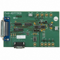
EVAL-AD7731EBZ
Manufacturer Part Number
EVAL-AD7731EBZ
Description
BOARD EVALUATION FOR AD7731
Manufacturer
Analog Devices Inc
Datasheets
1.AD7731BRUZ.pdf
(44 pages)
2.EVAL-AD7731EBZ.pdf
(11 pages)
3.EVAL-AD7731EBZ.pdf
(3 pages)
4.EVAL-AD7731EBZ.pdf
(44 pages)
Specifications of EVAL-AD7731EBZ
Number Of Adc's
1
Number Of Bits
24
Sampling Rate (per Second)
6.4k
Data Interface
Serial
Inputs Per Adc
3 Differential
Input Range
±1.28 V
Power (typ) @ Conditions
67.5mW @ 6.4kSPS
Voltage Supply Source
Analog and Digital
Operating Temperature
-40°C ~ 85°C
Utilized Ic / Part
AD7731
Lead Free Status / RoHS Status
Lead free / RoHS Compliant


Link Options (ctnd)
Link No.
LK9
LK10
LK11
SETUP CONDITIONS
Table I shows the position in which all the links are set
when the evaluation board is sent out.
Table I. Initial Link Positions
Link No. Position
LK1
LK2
LK3
LK4
LK5
LK6
LK7
LK8
LK9
LK10
LK11
EVALUATION BOARD INTERFACING
Interfacing to the evaluation board is either via a 9-way D-
Type connector, SKT1, or a 36-way Centronics connec-
tor, SKT2. The pinout for the SKT1 connector is given in
Figure 1 and its corresponding pin designations are given
in Table II. The pinout for this SKT2 connector is shown
in Figure 2 and its pin designations are given in Table III.
The evaluation board should be powered up before a cable
is connected to either of the connectors.
SKT2 is used to connect the evaluation board to the printer
port (parallel port) of a PC. Connection between the two
is direct via a standard parallel printer port cable. SKT1
is used to connect the evaluation board to any other system.
REV. A
B
A
B
A
A
I N
I N
I N
I N
I N
I N
Function
This link is in series with the AIN4/D0 pin.
With this link in place, SKT6 is connected directly to the AIN4/D0 pin.
This link may be removed so that an analog input signal at SKT6 can be connected to the component grid for
signal conditioning before being applied to the AIN4 input of the AD7731.
This link is in series with the AIN1 analog input.
With this link in place, the analog input on the SKT3 input is connected directly to the AIN1 input on the part.
This link may be removed so that the input signal at SKT3 can be connected to the component grid for signal
conditioning before being applied to the AIN1 input of the AD7731.
This link is in series with the AIN2 analog input.
With this link in place, the analog input on the SKT4 input is connected directly to the AIN2 input on the part.
This link may be removed so that the input signal at SKT4 can be connected to the component grid for signal
conditioning before being applied to the AIN2 input of the AD7731.
Function.
on-board crystal oscillator as the mas-
ter clock for the board.
AGND.
Both links in position B to select the
Normal Operating Mode.
REF IN(-) connected directly to
POL pin of AD7731 tied high.
REF IN(+) connected to the AD780.
SKT7 connected to AIN5.
SKT8 connected to AIN6.
SKT5 connected to AIN3/D1.
SKT6 connected to AIN4/D0.
SKT3 connected to AIN1.
SKT4 connected to AIN2.
–3–
Table II. SKT1 Pin Designations
1
2
3
4
5
6
7
8
9
N O T E
1
III as part of the SKT2 pin designations description.
An explanation of the AD7731 functions mentioned here is given in Table
SCLK
D I N
D G N D
D O U T
DV
N C
DD
Figure 2. SKT1 Pin Configuration
1
Serial Clock. The signal on this pin is buff-
ered before being applied to the SCLK pin of
the AD7731.
Logic Output. This is a buffered version of
the signal on the AD7731's
Chip Select. The signal on this pin is buffered
before being applied to the
AD7731.
Reset Input. The signal on this pin is buffered
before being applied to the
AD7731.
Serial Data Input. Data applied to this pin is
buffered before being applied to the AD7731's
DIN pin.
Ground reference point for digital circuitry.
Connects to the DGND plane on the evalua-
tion board.
Serial Data Output. This is a buffered version
of the signal on the AD7731's DOUT pin.
Digital Supply Voltage. The DV
for the evaluation board can be supplied via
this pin provided no voltage is applied to the
main DV
No Connect. The signal on this pin is buff-
ered before being applied to the
the AD7731.
6
2
7
DD
EVAL-AD7731EB
3
terminal.
8
1
4
9
5
pin of the
DD
pin.
pin of the
voltage
pin of
Related parts for EVAL-AD7731EBZ
Image
Part Number
Description
Manufacturer
Datasheet
Request
R


Part Number:
Description:
BOARD EVAL FOR SI270X-A
Manufacturer:
Silicon Laboratories Inc
Datasheet:

Part Number:
Description:
BUCK CONV REF DESIGN KIT IP1201
Manufacturer:
International Rectifier
Datasheet:
Part Number:
Description:
BOARD DEMO SYNC DUAL BUCK CNVTER
Manufacturer:
International Rectifier
Datasheet:
Part Number:
Description:
BOARD DEMO SYNC BUCK CONVETER
Manufacturer:
International Rectifier
Datasheet:

Part Number:
Description:
EVALBOARD/EB Omnidirectional microphone - Analog
Manufacturer:
Analog Devices
Datasheet:
Part Number:
Description:
EVALBOARD/EB Omnidirectional microphone - Analog
Manufacturer:
Analog Devices
Datasheet:


Part Number:
Description:
BOARD EVAL LED DRIVER LT3756
Manufacturer:
Linear Technology
Datasheet:

Part Number:
Description:
BOARD EVAL FOR AD7741/7742
Manufacturer:
Analog Devices Inc
Datasheet:

Part Number:
Description:
±1.7g Dual-Axis IMEMS Accelerometer Evaluation Board
Manufacturer:
Analog Devices Inc
Datasheet:

Part Number:
Description:
IC MULTIPLIER ANALOG 8-SOIC T/R
Manufacturer:
Analog Devices Inc
Datasheet:

Part Number:
Description:
IC ANALOG MULTIPLIER 8-DIP
Manufacturer:
Analog Devices Inc
Datasheet:
Part Number:
Description:
IC ANALOG MULTIPLIER 8-SOIC
Manufacturer:
Analog Devices Inc
Datasheet:
Part Number:
Description:
IC ANALOG MULTIPLIER 8-DIP
Manufacturer:
Analog Devices Inc
Datasheet: