AD9262-10EBZ Analog Devices Inc, AD9262-10EBZ Datasheet - Page 5
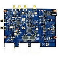
AD9262-10EBZ
Manufacturer Part Number
AD9262-10EBZ
Description
BOARD EVALUATION 10MHZ AD9262
Manufacturer
Analog Devices Inc
Specifications of AD9262-10EBZ
Design Resources
Interfacing ADL5382 to AD9262 as an RF-to-Bits Solution (CN0062)
Number Of Adc's
2
Number Of Bits
16
Sampling Rate (per Second)
160M
Data Interface
Serial, SPI™
Inputs Per Adc
1 Differential
Input Range
2 Vpp
Power (typ) @ Conditions
600mW @ 40MSPS
Voltage Supply Source
Analog and Digital
Operating Temperature
-40°C ~ 85°C
Utilized Ic / Part
AD9262
Silicon Manufacturer
Analog Devices
Application Sub Type
ADC
Kit Application Type
Data Converter
Silicon Core Number
AD9262
Kit Contents
Software, Evaluation Board
Lead Free Status / RoHS Status
Lead free / RoHS Compliant


Evaluation Board User Guide
CONFIGURING THE EVALUATION BOARD
POWER SUPPLY
Power is provided to the evaluation board by a single +6.0 V
source applied to P2. The power source is regulated down to the
appropriate levels by the ADP3339 voltage regulators. Table 3
shows the necessary voltage levels for each component.
Table 3. Component Power Supplies
Component
AD9262
ADL5382
AD9516-0
CLOCK
The AD9262 evaluation board offers many clocking options:
a high frequency external clock can be applied directly to the
ADC; the AD9516-0 LVPECL or CMOS clock can be used; and
a low frequency clock, in conjunction with the integrated PLL
from either the AD9516-0 or AD9262, can provide the necessary
input clock frequency. The default clock option is configured
for an external clock rate of 640 MHz.
The AD9262 evaluation board includes the footprint for a Valpey
Fisher VFAC3 crystal oscillator. The crystal oscillator can serve
as the reference clock to the AD9516-0, and the chip’s internal
PLL can be used to generate a clock closest to the desired fre-
quency for the ADC. For example, a 122.88 MHz reference
produces a VCO frequency of 2.580 GHz. The AD9516-0
possesses an integrated VCO. The VCO frequency is further
divided down by 4 to generate an output clock of 645 MHz,
which serves as the input clock to the ADC. To optimize the
AD9516-0 for this particular frequency, the loop filter must be
configured as shown in Figure 5.
If the user chooses an alternative crystal oscillator frequency,
the loop filter components must be configured appropriately.
Some common crystal oscillators and the corresponding loop
filter components are shown in Table 4. Refer to the ADIsimCLK
software for design guidance.
Table 4. AD9516-0 CLK Configuration
Crystal
(MHz)
134.4
122.88
39.3216 1500 pF 221 Ω
C107
1000 pF 232 Ω
1000 pF 280 Ω
CP
1000pF
C107
0Ω
R11
Figure 5. AD9516-0 Loop Filter
Loop Filter
C31
18,000 pF 486 Ω 680 pF
15,000 pF 576 Ω 560 pF
22,000 pF 453 Ω 680 pF
R11
280Ω
C31
15,000pF
576Ω
R13
Power Supply
1.8 V
5.0 V
3.3 V
C108
560pF
R19
R13
0Ω
LF
BYPASS_LDO
C108
AD9262
CLK
672
645.12
648.8
MHz
MHz
MHz
Rev. 0 | Page 5 of 24
To configure the evaluation board for either the external clock
source or the AD9516-0 requires modifying the JP5 and JP6
solder jumpers. The AD9262 sets the common-mode level of
the input clock to 450 mV; therefore, the clock source should be
ac-coupled to the ADC input clock pins. Use the AD9516-0
software to configure the chip to the appropriate divide ratios.
RECEIVER INPUT CONFIGURATION
The default configuration uses the complex output signals of
the I/Q demodulator as the input signals to the AD9262. In this
configuration, the RF input signal should be applied to J2 and
the LO signal to J1. The RF input range of the ADL5382 is
limited to between 700 MHz and 2.7 GHz. The single-ended
RF and LO signals are converted to differential signals using the
RF transformers, T2 and T1. The resulting output signals of the
demodulator are differential I and Q signals that can be directly
applied to the resistive inputs of the AD9262, and no driver
amplifiers are required.
Between the output of the ADL5382 and the input to the
AD9262 are space holders for a fourth order filter (see Figure 6).
This filter may or may not be necessary depending on the
application.
ADC ONLY INPUT CONFIGURATION
In addition to using the ADL5382 as an input source to the
ADC, the AD9262 can be driven with an external source through
either the ADA4937 or a differential transformer.
To configure the evaluation board for an external source, follow
the hardware configuration shown in Table 5. The SMA
connectors, labeled J5 and J4, correspond to the input signals to
Channel A and Channel B, respectively, of the AD9262.
Additionally, short TP17, TP23, TP2, and TP24 to the appropriate
pads to route the external signals to the input pins of the AD9262
(see Figure 7). This configuration requires careful attention to
ensure that the output signals of the ADL5382 are disconnected
and only the signals from the transformer or ADA4937 are
routed to the ADC.
L3
L4
Figure 6. Fourth Order Filter
L7
L8
C48
L11
L12
L15
L16
C50
UG-051
Related parts for AD9262-10EBZ
Image
Part Number
Description
Manufacturer
Datasheet
Request
R

Part Number:
Description:
BOARD EVALUATION 5MHZ AD9262
Manufacturer:
Analog Devices Inc
Datasheet:
Part Number:
Description:
BOARD EVALUATION FOR AD9262
Manufacturer:
Analog Devices Inc
Datasheet:

Part Number:
Description:
±1.7g Dual-Axis IMEMS Accelerometer Evaluation Board
Manufacturer:
Analog Devices Inc
Datasheet:

Part Number:
Description:
Inertial Sensor Evaluation System
Manufacturer:
Analog Devices Inc
Datasheet:
Part Number:
Description:
Manufacturer:
Analog Devices Inc
Datasheet:
Part Number:
Description:
Manufacturer:
Analog Devices Inc
Datasheet:
Part Number:
Description:
Manufacturer:
Analog Devices Inc
Datasheet:
Part Number:
Description:
Manufacturer:
Analog Devices Inc
Datasheet:
Part Number:
Description:
Manufacturer:
Analog Devices Inc
Datasheet:
Part Number:
Description:
Manufacturer:
Analog Devices Inc
Datasheet:
Part Number:
Description:
Manufacturer:
Analog Devices Inc
Datasheet:
Part Number:
Description:
Manufacturer:
Analog Devices Inc
Datasheet:
Part Number:
Description:
Manufacturer:
Analog Devices Inc
Datasheet: