SSM2305-EVALZ Analog Devices Inc, SSM2305-EVALZ Datasheet - Page 4
SSM2305-EVALZ
Manufacturer Part Number
SSM2305-EVALZ
Description
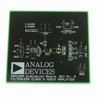
BOARD EVAL FOR SSM2305 LFCSP
Manufacturer
Analog Devices Inc
Specifications of SSM2305-EVALZ
Amplifier Type
Class D
Output Type
1-Channel (Mono)
Max Output Power X Channels @ Load
2.8W x 1 @ 4 Ohm
Voltage - Supply
2.2 V ~ 5.5 V
Operating Temperature
-40°C ~ 85°C
Board Type
Fully Populated
Utilized Ic / Part
SSM2305
Silicon Manufacturer
Analog Devices
Application Sub Type
Audio Power Amplifier - Class D
Kit Application Type
Amplifier
Silicon Core Number
SSM2305
Kit Contents
Board
Lead Free Status / RoHS Status
Lead free / RoHS Compliant


EVAL-SSM2305
Table 1. Recommended Output Beads (L1 and L2)
Part No.
BLM18PG121SN1D
MPZ1608S101A
MPZ1608S221A
BLM18EG221SN1D
Table 2. Recommended Output Inductors (L3 and L4)
Part No.
LQM31PNR47M00
LQM31PN1R0M00
LQM21PNR47MC0
LQM21PN1R0MC0
LQH32CN2R2M53
Ensure that these beads have enough current conducting capability
while providing sufficient EMI attenuation. The current rating
needed for an 8 Ω load is approximately 420 mA, and impedance
at 100 MHz must be ≥120 Ω. In addition, the lower the dc resis-
tance (DCR) of these beads, the better for minimizing their
power consumption. Table 1 describes the recommended beads.
Output Shunting Capacitors—C3, C4, C8 and C9
There are two output shunting capacitors, C8 and C9, that work
with the F1 and F2 ferrite beads. There are also two output
shunting capacitors, C3 and C4, that work with the L1 and L2
inductors, if they are used. Use small size (0603 or 0402) multi-
layer ceramic capacitors that are made of X7R or COG (NPO)
materials. Note that the capacitors can be used in pairs: a capa-
citor with small capacitance (up to 100 pF) plus a capacitor with
a larger capacitance (less than 1 nF). This configuration provides
thorough EMI reduction for the entire frequency spectrum. For
BOM cost reduction and capable performance, a single capacitor
of approximately 470 pF can be used.
Output Inductors
If you prefer using inductors for the purpose of EMI filtering
at the output nodes, choose inductance that is <2.2 μH. The
higher the inductance, the lower the EMI is at the output.
However, the cost and power consumption by the inductors are
higher. Using 0.47 μH to 2.2 μH inductors is recommended, and
the current rating needs >600 mA (satur-ation current) for an
8 Ω load. Table 2 shows the recommended inductors. Note that
these inductors are not populated on the evaluation board.
PCB LAYOUT GUIDELINES
To lay out the board, do the following:
1.
2.
In the LFCSP package, place at least nine vias on the solder
pad for the thermal pad of the amplifier for proper
conduction of heat to the opposite side of the board.
The outer diameter of the vias should be 0.5 mm, and the
inner diameter should be 0.25 mm to 0.3 mm.
Use a PCB area of at least 2 cm
opposite side of the layer of the amplifier chip as a heat
Manufacturer
Murata
TDK
TDK
Murata
Manufacturer
Murata
Murata
Murata
Murata
Murata
2
equivalent area on the
Rev. 0 | Page 4 of 8
Z (Ω)
120
100
220
220
0.47
0.47
L (μH)
1.0
1.0
2.2
3.
4.
5.
Figure 5. Correct Placement and Routing for Decoupling Capacitors
sink. Also, extend the ground pad (for the thermal pad) as
much as possible on the amplifier side of the PCB as a heat
sink (see Figure 4).
If internal layers are available, allocate a certain area as a heat
sink; make sure to connect the vias conducting the heat to
the internal layers.
Place the EMI filtering beads, F1 and F2, as close to the
amplifier chip as possible.
Place the decoupling capacitors for the C8 and C9 beads as
close to the amplifier chip as possible, and connect all their
ground terminals together, as close as possible.
Ideally, solder their ground terminals together, as shown in
Figure 5. Do not rely on PCB tracks or ground planes for
connecting these ground terminals.
I
1400
1200
1100
800
790
I
2000
3000
2000
2000
MAX
MAX
COPPER
(mA)
FILL
(mA)
INDUCTOR
SMALL
C12
Figure 4. Heat Sink Layout
C8
C9
0.05
0.03
0.05
0.05
DCR (Ω)
0.07
0.12
0.12
0.19
0.1
DCR (Ω)
C10
C13
C11
TOP LAYER
INTERNAL
AND/OR
BOTTOM LAYER
Size (mm)
1.6 × 0.8 × 0.8
1.6 × 0.8 × 0.8
1.6 × 0.8 × 0.8
1.6 × 0.8 × 0.8
Size (mm)
3.2 × 1.6 × 0.85
3.2 × 1.6 × 0.85
2.0 × 1.25 × 0.5
2.0 × 1.25 × 0.5
3.2 × 2.5 × 1.55
OUTPUT
TRACK
INPUT
TRACK
Related parts for SSM2305-EVALZ
Image
Part Number
Description
Manufacturer
Datasheet
Request
R

Part Number:
Description:
±1.7g Dual-Axis IMEMS Accelerometer Evaluation Board
Manufacturer:
Analog Devices Inc
Datasheet:

Part Number:
Description:
Inertial Sensor Evaluation System
Manufacturer:
Analog Devices Inc
Datasheet:
Part Number:
Description:
Manufacturer:
Analog Devices Inc
Datasheet:
Part Number:
Description:
Manufacturer:
Analog Devices Inc
Datasheet:
Part Number:
Description:
Manufacturer:
Analog Devices Inc
Datasheet:
Part Number:
Description:
Manufacturer:
Analog Devices Inc
Datasheet:
Part Number:
Description:
Manufacturer:
Analog Devices Inc
Datasheet:
Part Number:
Description:
Manufacturer:
Analog Devices Inc
Datasheet:
Part Number:
Description:
Manufacturer:
Analog Devices Inc
Datasheet:
Part Number:
Description:
Manufacturer:
Analog Devices Inc
Datasheet:
Part Number:
Description:
Manufacturer:
Analog Devices Inc
Datasheet:
Part Number:
Description:
Manufacturer:
Analog Devices Inc
Datasheet:
Part Number:
Description:
Manufacturer:
Analog Devices Inc
Datasheet: