LM5118EVAL/NOPB National Semiconductor, LM5118EVAL/NOPB Datasheet - Page 19
LM5118EVAL/NOPB
Manufacturer Part Number
LM5118EVAL/NOPB
Description
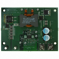
BOARD EVALUATION FOR LM5118
Manufacturer
National Semiconductor
Series
PowerWise®r
Specifications of LM5118EVAL/NOPB
Main Purpose
DC/DC, Step Up or Down
Outputs And Type
1, Non-Isolated
Voltage - Output
12V
Current - Output
3A
Voltage - Input
5 ~ 75V
Regulator Topology
Buck-Boost
Frequency - Switching
300kHz
Board Type
Fully Populated
Utilized Ic / Part
LM5118
Lead Free Status / RoHS Status
Not applicable / Not applicable
Power - Output
-
Other names
*LM5118EVAL
LM5118EVAL
LM5118EVAL


and assumes a current limit>Iload + ICout
For this application, a C16 value of 0.1 µF was chosen which
corresponds to a soft-start time of about 12 ms.
R8, R9
R8 and R9 set the output voltage level, the ratio of these re-
sistors is calculated from:
For a 12V output, the R8/R9 ratio calculates to 9.76. The re-
sistors should be chosen from standard value resistors and a
good starting point is to select resistors within power ratings
appropriate for the output voltage. Values of 309Ω for R9 and
2.67 kΩ for R8 were selected.
R1, R3, C21
A voltage divider can be connected to the UVLO pin to set a
minimum operating voltage VIN
feature is required, the easiest approach to select the divider
resistor values is to choose a value for R1 between 10 kΩ and
100 kΩ, while observing the minimum value of R1 necessary
to allow the UVLO switch to pull the UVLO pin low. This value
is:
R1
R1
R3 is then calculated from
Since VIN
some margin in component tolerances and input ripple.
R1 = 75k is chosen since it is a standard value
R3 = 29.332k is calculated from the equation above. 29.4k
was used since it is a standard value.
Capacitor C21 provides filtering for the divider and the off time
of the “hiccup” duty cycle during current limit. The voltage at
the UVLO pin should never exceed 15V when using an ex-
ternal set-point divider. It may be necessary to clamp the
UVLO pin at high input voltages.
Knowing the desired off time during “hiccup” current limit, the
value of C21 is given by:
Notice that t
In this example, C21 was chosen to be 0.1 µF. This will set
the t
R2
A 1M pull-up resistor connected from the EN pin to the VIN
pin is sufficient to keep enable in a high state if on-off control
is not used.
≥
≥
OFF
1000 x V
75k in our example
time to 956 µs with VIN = 12V.
(MIN)
OFF
IN(MAX)
for our example is 5V, set VIN
varies with V
IN
(UVLO)
for the regulator. If this
(UVLO)
to 4.0V for
19
SNUBBER
A snubber network across the buck re-circulating diode re-
duces ringing and spikes at the switching node. Excessive
ringing and spikes can cause erratic operation and increase
noise at the regulator output. In the limit, spikes beyond the
maximum voltage rating of the LM5118 or the re-circulating
diode can damage these devices. Selecting the values for the
snubber is best accomplished through empirical methods.
First, make sure the lead lengths for the snubber connections
are very short. Start with a resistor value between 5 and 20
Ohms. Increasing the value of the snubber capacitor results
in more damping, however the snubber losses increase. Se-
lect a minimum value of the capacitor that provides adequate
clamping of the diode waveform at maximum load. A snubber
may be required for the boost diode as well. The same em-
pirical procedure applies. Snubbers were not necessary in
this example.
Error Amplifier Configuration
R4, C18, C17
These components configure the error amplifier gain charac-
teristics to accomplish a stable overall loop gain. One advan-
tage of current mode control is the ability to close the loop with
only three feedback components, R4, C18 and C17. The
overall loop gain is the product of the modulator gain and the
error amplifier gain. The DC modulator gain of the LM5118 is
as follows:
The dominant, low frequency pole of the modulator is deter-
mined by the load resistance (R
(C
For this example, R
µF, therefore:
f
DC Gain
Additionally, there is a right-half plane (RHP) zero associated
with the modulator. The frequency of the RHP zero is:
f
The output capacitor ESR produces a zero given by:
ESR
The RHP zero complicates compensation. The best design
approach is to reduce the loop gain to cross zero at about
30% of the calculated RHP zero frequency. The Type ll error
amplifier compensation provided by R4, C18 and C17 places
one pole at the origin for high DC gain. The 2nd pole should
P(MOD)
RHPzero
OUT
ZERO
). The corner frequency of this pole is:
= 149 Hz
= 7.8 kHz
(MOD)
= 70 kHz
=3.63 = 11.2 dB
LOAD
= 4Ω, D
LOAD
MIN
) and output capacitance
= 0.294, and C
www.national.com
OUT
= 454
Related parts for LM5118EVAL/NOPB
Image
Part Number
Description
Manufacturer
Datasheet
Request
R

Part Number:
Description:
National Semiconductor [8-Bit D/A Converter]
Manufacturer:
National Semiconductor
Datasheet:
Part Number:
Description:
National Semiconductor [Media Coprocessor]
Manufacturer:
National Semiconductor
Datasheet:
Part Number:
Description:
Digitally Controlled Tone and Volume Circuit with Stereo Audio Power Amplifier, Microphone Preamp Stage and National 3D Sound
Manufacturer:
National Semiconductor
Datasheet:
Part Number:
Description:
Digitally Controlled Tone and Volume Circuit with Stereo Audio Power Amplifier, Microphone Preamp Stage and National 3D Sound
Manufacturer:
National Semiconductor
Datasheet:
Part Number:
Description:
AC97 Rev 2 Codec with Sample Rate Conversion and National 3D Sound
Manufacturer:
National Semiconductor
Part Number:
Description:
Manufacturer:
National Semiconductor
Datasheet:
Part Number:
Description:
Manufacturer:
National Semiconductor
Datasheet:
Part Number:
Description:
General Purpose, Low Voltage, Low Power, Rail-to-Rail Output Operational Amplifiers
Manufacturer:
National Semiconductor
Datasheet:
Part Number:
Description:
8-bit 20 MSPS flash A/D converter.
Manufacturer:
National Semiconductor
Datasheet:
Part Number:
Description:
Low Noise Quad Operational Amplifier
Manufacturer:
National Semiconductor
Datasheet:
Part Number:
Description:
Quad Differential Line Receivers
Manufacturer:
National Semiconductor
Datasheet:
Part Number:
Description:
Quad High Speed Trapezoidal? Bus Transceiver
Manufacturer:
National Semiconductor
Datasheet:
Part Number:
Description:
Dual Line Receiver
Manufacturer:
National Semiconductor
Datasheet:
Part Number:
Description:
TTL to 10k ECL Level Translator with Latch
Manufacturer:
National Semiconductor
Datasheet: