LM5118EVAL/NOPB National Semiconductor, LM5118EVAL/NOPB Datasheet - Page 2
LM5118EVAL/NOPB
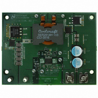
Manufacturer Part Number
LM5118EVAL/NOPB
Description
BOARD EVALUATION FOR LM5118
Manufacturer
National Semiconductor
Series
PowerWise®r
Specifications of LM5118EVAL/NOPB
Main Purpose
DC/DC, Step Up or Down
Outputs And Type
1, Non-Isolated
Voltage - Output
12V
Current - Output
3A
Voltage - Input
5 ~ 75V
Regulator Topology
Buck-Boost
Frequency - Switching
300kHz
Board Type
Fully Populated
Utilized Ic / Part
LM5118
Lead Free Status / RoHS Status
Not applicable / Not applicable
Power - Output
-
Other names
*LM5118EVAL
LM5118EVAL
LM5118EVAL


www.national.com
Ordering Number
Connection Diagram
Ordering Information
*Automotive Grade (Q) product incorporates enhanced manufacturing and support processes for the automotive market, including defect detection methodologies.
Reliability qualification is compliant with the requirements and temperature grades defined in the AEC-Q100 standard. Automotive grade products are identified
with the letter Q. For more information go to http://www.national.com/automotive.
Pin Descriptions
LM5118Q1MHX
LM5118Q1MH
LM5118MHX
Pin
LM5118MH
10
1
2
3
4
5
6
7
8
9
COMP
RAMP
AGND
VOUT
Name
UVLO
VIN
EN
RT
SS
FB
Description
Input supply voltage.
If the UVLO pin is below 1.23V, the regulator will be in standby mode (VCC regulator running, switching
regulator disabled). When the UVLO pin exceeds 1.23V, the regulator enters the normal operating mode. An
external voltage divider can be used to set an under-voltage shutdown threshold. A fixed 5 µA current is sourced
out of the UVLO pin. If a current limit condition exists for 256 consecutive switching cycles, an internal switch
pulls the UVLO pin to ground and then releases.
The internal oscillator frequency is set with a single resistor between this pin and the AGND pin. The
recommended frequency range is 50 kHz to 500 kHz.
If the EN pin is below 0.5V, the regulator will be in a low power state drawing less than 10 µA from VIN. EN
must be raised above 3V for normal operation.
Ramp control signal. An external capacitor connected between this pin and the AGND pin sets the ramp slope
used for emulated current mode control.
Analog ground.
Soft-Start. An external capacitor and an internal 10 µA current source set the rise time of the error amp
reference. The SS pin is held low when VCC is less than the VCC under-voltage threshold (< 3.7V), when the
UVLO pin is low (< 1.23V), when EN is low (< 0.5V) or when thermal shutdown is active.
Feedback signal from the regulated output. Connect to the inverting input of the internal error amplifier.
Output of the internal error amplifier. The loop compensation network should be connected between COMP
and the FB pin.
Output voltage monitor for emulated current mode control. Connect this pin directly to the regulated output.
Package Type
TSSOP-20EP
TSSOP-20EP
TSSOP-20EP
TSSOP-20EP
NSC Package
See NS Package Numbers MXA20A
Drawing
MXA20A
MXA20A
MXA20A
MXA20A
Top View
2500 units shipped as Tape & Reel
2500 units shipped as Tape & Reel
2
73 Units Per Anti-Static Tube
73 Units Per Anti-Static Tube
Supplied As
30058502
AEC-Q100 Grade 1 qualified.
Automotive Grade Production
Feature
Flow*
Related parts for LM5118EVAL/NOPB
Image
Part Number
Description
Manufacturer
Datasheet
Request
R

Part Number:
Description:
National Semiconductor [8-Bit D/A Converter]
Manufacturer:
National Semiconductor
Datasheet:
Part Number:
Description:
National Semiconductor [Media Coprocessor]
Manufacturer:
National Semiconductor
Datasheet:
Part Number:
Description:
Digitally Controlled Tone and Volume Circuit with Stereo Audio Power Amplifier, Microphone Preamp Stage and National 3D Sound
Manufacturer:
National Semiconductor
Datasheet:
Part Number:
Description:
Digitally Controlled Tone and Volume Circuit with Stereo Audio Power Amplifier, Microphone Preamp Stage and National 3D Sound
Manufacturer:
National Semiconductor
Datasheet:
Part Number:
Description:
AC97 Rev 2 Codec with Sample Rate Conversion and National 3D Sound
Manufacturer:
National Semiconductor
Part Number:
Description:
Manufacturer:
National Semiconductor
Datasheet:
Part Number:
Description:
Manufacturer:
National Semiconductor
Datasheet:
Part Number:
Description:
General Purpose, Low Voltage, Low Power, Rail-to-Rail Output Operational Amplifiers
Manufacturer:
National Semiconductor
Datasheet:
Part Number:
Description:
8-bit 20 MSPS flash A/D converter.
Manufacturer:
National Semiconductor
Datasheet:
Part Number:
Description:
Low Noise Quad Operational Amplifier
Manufacturer:
National Semiconductor
Datasheet:
Part Number:
Description:
Quad Differential Line Receivers
Manufacturer:
National Semiconductor
Datasheet:
Part Number:
Description:
Quad High Speed Trapezoidal? Bus Transceiver
Manufacturer:
National Semiconductor
Datasheet:
Part Number:
Description:
Dual Line Receiver
Manufacturer:
National Semiconductor
Datasheet:
Part Number:
Description:
TTL to 10k ECL Level Translator with Latch
Manufacturer:
National Semiconductor
Datasheet: