MCP1640EV-SBC Microchip Technology, MCP1640EV-SBC Datasheet - Page 11
MCP1640EV-SBC
Manufacturer Part Number
MCP1640EV-SBC
Description
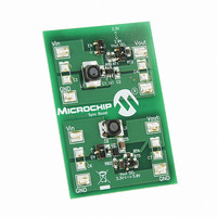
BOARD EVAL FOR MCP1640
Manufacturer
Microchip Technology
Type
DC/DC Switching Converters, Regulators & Controllersr
Datasheets
1.MCP1640CT-ICHY.pdf
(32 pages)
2.MCP1640CT-ICHY.pdf
(26 pages)
3.MCP1640EV-SBC.pdf
(22 pages)
Specifications of MCP1640EV-SBC
Main Purpose
DC/DC, Step Up
Outputs And Type
1, Non-Isolated
Voltage - Output
2V, 3.3V or 5V
Current - Output
100mA, 350mA
Voltage - Input
0.35 ~ 5.5V
Regulator Topology
Boost
Frequency - Switching
500kHz
Board Type
Fully Populated
Utilized Ic / Part
MCP1640
Input Voltage
0.35 V to 5.5 V
Output Voltage
3.3 V to 5 V
Operating Supply Voltage
0.35 V to 5.5 V
Product
Power Management Modules
Supply Current
300 mA
Kit Contents
Board
Features
Automatic PFM/PWM Operation, Enable State Selectable Using Mini-Dip Switch On Board
Svhc
No SVHC (15-Dec-2010)
Core Architecture
Power Management - Voltage Regulator
Rohs Compliant
Yes
For Use With/related Products
MCP1640
Lead Free Status / RoHS Status
Contains lead / RoHS non-compliant
Power - Output
-
Lead Free Status / Rohs Status
Lead free / RoHS Compliant
Available stocks
Company
Part Number
Manufacturer
Quantity
Price
Company:

Part Number:
MCP1640EV-SBC
Manufacturer:
Microchip Technology
Quantity:
135
Company:
Part Number:
MCP1640EV-SBC
Manufacturer:
MICROCHIP
Quantity:
12 000


2.1
FIGURE 2-1:
2010 Microchip Technology Inc.
GND
V
IN
+
_
INTRODUCTION
P1
1
1
10 µF
C
P1
1
Chapter 2. Installation and Operation
S1
The MCP1640 is a compact, high-efficiency, fixed frequency, synchronous step-up
dc-dc converter. It provides an easy-to-use power supply solution for applications
powered by one-cell, two-cell, or three-cell alkaline, NiCd, NiMH, one-cell Li-Ion or
Li-Polymer batteries in addition to distributed 3.3V to 5.0V applications.
The MCP1640 is capable of regulating the output voltage over a wide 2.0V to 5.5V
range and typically can deliver over 100 mA of load current at 3.3V output when
supplied from a single 1.2V cell. The input voltage range is 0.35V to 5.5V with a low
0.65V start-up voltage. The regulated output voltage, V
equal to the input voltage, V
transition to optimize efficiency, low device quiescent current (20 µA in PFM mode and
1 µA in stand-by mode), multiple and selectable, logic controlled shutdown states (true
load disconnect or “bypass”, output connected to input), low noise and discontinuous
current anti-ring control.
MCP1640 Synchronous Boost SOT-23-6 Application.
Two enable mode options are available: true disconnect and bypass. When disabled,
the true disconnect option removes the normal boost topology path from input to output
by opening the diode path using a P-Channel synchronous switch with a reversible
body diode. The bypass option uses the synchronous boost converter P-Channel
switch to connect the input to the output through the boost inductor while disabled
providing voltage to the load, while consuming less than 1 µA of current from V
The MCP1640 is available in SOT-23-6 and 2x3 mm DFN-8 lead packages.
EN Switch
P1
CONVERTER EVALUATION BOARD
1
2
3
MCP1640 SYNCHRONOUS BOOST
Note: Calculate RT resistors
RT = RB * ((V
V
SW
GND
EN
L
FB
1
MCP1640
SOT-23-6
= 1.21V
for a particular V
U1
IN
V
4,7 µH
OUT
V
OUT
. Additional device features are: automatic PWM / PFM
FB
IN
/ V
6
5
4
FB
OUT
) -1)
as:
V
OUT
3.3V
309 k
RB
OUT
SEL
1
USER’S GUIDE
should be greater than or
2.0V
S1
P1
DS51880A-page 11
10 µF
C
2
1
1
P1
+
_
IN
V
GND
.
OUT
Related parts for MCP1640EV-SBC
Image
Part Number
Description
Manufacturer
Datasheet
Request
R

Part Number:
Description:
0.65V Start-up Synchronous Boost Regulator with True Output Disconnect or Input/Output Bypass Option
Manufacturer:
MICROCHIP [Microchip Technology]
Datasheet:

Part Number:
Description:
IC CONV DC-DC STEPUP SYNC 8DFN
Manufacturer:
Microchip Technology
Datasheet:

Part Number:
Description:
0.65v Start-up Synchronous Boost Regulator With True Output Disconnect Or Input/output Bypass Option
Manufacturer:
Microchip Technology Inc.
Datasheet:
Part Number:
Description:
Manufacturer:
Microchip Technology Inc.
Datasheet:
Part Number:
Description:
Manufacturer:
Microchip Technology Inc.
Datasheet:
Part Number:
Description:
Manufacturer:
Microchip Technology Inc.
Datasheet:
Part Number:
Description:
Manufacturer:
Microchip Technology Inc.
Datasheet:
Part Number:
Description:
Manufacturer:
Microchip Technology Inc.
Datasheet:
Part Number:
Description:
Manufacturer:
Microchip Technology Inc.
Datasheet:
Part Number:
Description:
Manufacturer:
Microchip Technology Inc.
Datasheet: